Reinforcing structure of radiation-resistant groove type MOS field effect transistor for satellite and preparation method

A field effect transistor and reinforcement structure technology, applied in the field of electronics, can solve problems such as insufficient radiation resistance

Active Publication Date: 2021-03-16
XIAN MICROELECTRONICS TECH INST
View PDF8 Cites 2 Cited by
  • Summary
  • Abstract
  • Description
  • Claims
  • Application Information

AI Technical Summary

Problems solved by technology

In the prior art, there is a shortcoming of insufficient rad

Method used


Image

  • Reinforcing structure of radiation-resistant groove type MOS field effect transistor for satellite and preparation method
  • Reinforcing structure of radiation-resistant groove type MOS field effect transistor for satellite and preparation method
  • Reinforcing structure of radiation-resistant groove type MOS field effect transistor for satellite and preparation method

Examples


preparation example Construction

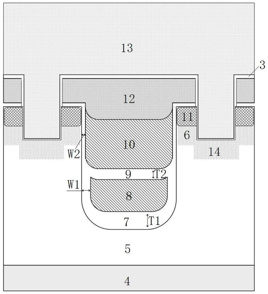
[0044] The invention relates to a reinforced structure and a preparation method of a radiation-resistant trench type MOS field effect transistor for satellites. The gate and source double-groove MOS field effect transistors are manufactured through a radiation-resistant process, which has better resistance to the total dose of ionization effects and single event effects. The reinforcement structure of the anti-radiation trench MOS field effect transistor for star use in the present invention aims at the radiation resistance requirement of the trench type MOS field effect transistor for star use, and proposes a double-groove radiation-resistant reinforcement unit structure, including gate trenches Groove and source trench, where the gate trench uses a deep trench shielded gate double-layer structure and a low-temperature trench gate oxidation process method for ionization total dose effect reinforcement; the source trench uses a shallow trench structure and P+ body region expans...

Embodiment

[0071] This embodiment adopts the unit structure of the double-groove MOS field effect transistor of the present invention to manufacture an N-type 100V power MOS field effect transistor device, and its specific process steps are as follows:

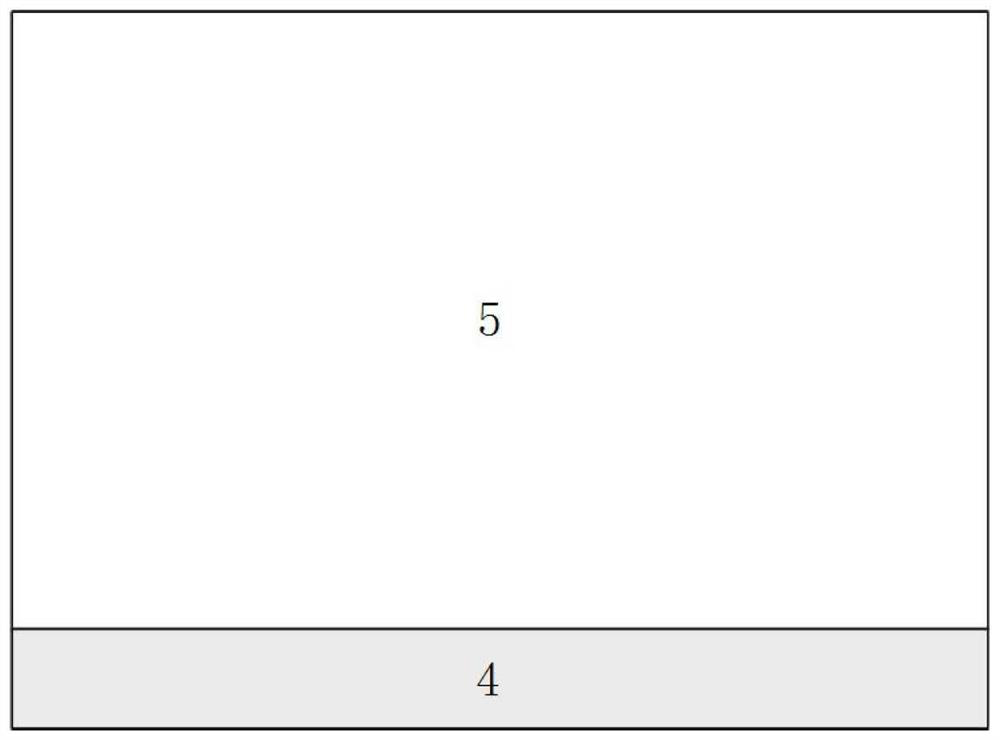
[0072] Step 1. If figure 2 As shown, the N silicon wafer with resistivity (0.002~0.003) Ω·cm is used as the substrate 4 material, and the requirements for three-layer epitaxial deposition are:

[0073] epitaxial layer Thickness (μm) Resistivity (Ω·cm) Epitaxy 1 18.0±2.0 0.15±0.01 Epitaxy 2 3.0±0.3 1.5±0.1 Epitaxy 3 10.0±0.8 2.50±0.3

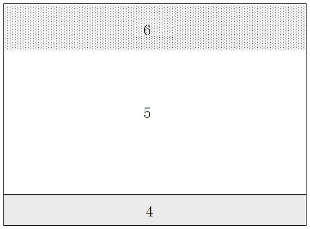
[0074] Step 2. The terminal adopts the structure combining the field limiting ring and the field plate, and the design withstand voltage is 120V. The lithography defines and uses 700nm field oxygen 1 as the mask layer, and 80KeV boron ion implantation forms the field limiting ring with a peak concentration of 3.0×10 15 cm -3 .

[0075] Step 3. Remove the field oxyg...


PUM

PropertyMeasurementUnit
Thicknessaaaaaaaaaa
Thicknessaaaaaaaaaa
Thicknessaaaaaaaaaa

Abstract

The invention discloses a reinforcing structure of a radiation-resistant groove type MOS field effect transistor for a satellite and a preparation method. The reinforcing structure comprises a substrate, a slowly-changing epitaxial layer, an interlayer dielectric layer and a metal layer which are stacked in sequence, a P+ body doped region and an N+ source doped region are sequentially arranged onthe surface of the slowly-changing epitaxial layer, and a gate trench is formed in the slowly-changing epitaxial layer; a first gate oxide, a floating polycrystalline gate, a second gate oxide and acontrol polycrystalline gate are sequentially stacked in the gate trench from bottom to top to form a double-layer shielding gate structure; the interlayer dielectric layer is provided with source shallow trenches, the source shallow trenches are symmetrically distributed at two sides of the gate trench, the source shallow trenches sequentially pass through the interlayer dielectric layer, the N+source doped region and the P+ body doped region, and the depth of the source shallow trenches does not exceed the longitudinal polycrystalline thickness of a control polycrystalline gate in the gatetrench; a P+ deep source is formed in each source shallow trench through ion implantation, wherein the P+ deep source is connected with the P+ body doped region; the metal layer is arranged on the interlayer dielectric layer and fills the source shallow trenches.

Description

technical field [0001] The invention belongs to the field of electronic technology, in particular to a reinforcement structure and a preparation method of a radiation-resistant trench type MOS field-effect transistor for satellites. Background technique [0002] Trench MOS field effect transistors use trench sidewalls to form the gate structure of the device, which effectively reduces the device JFET resistance and drain resistance, and increases the cell density of the gate structure; it has a lower conductivity than the planar gate MOS field effect transistor. On-resistance, better quality factor, faster switching rate and lower drive loss, more suitable for low power consumption and high current design requirements of new distributed power systems in satellites and space vehicles, higher unit density is conducive to Power module integration and system miniaturization. [0003] However, the radiation resistance of the existing trench type MOS field effect transistor is in...

Claims


Application Information

Patent Timeline
IPC IPC(8): H01L29/06H01L29/08H01L29/786H01L21/336H01L29/423
CPCH01L29/0623H01L29/0847H01L29/0657H01L29/0634H01L29/78633H01L29/78621H01L29/66742H01L29/4236H01L29/42376
Inventor 王晨杰王英民刘存生薛智民孙有民王小荷
Owner XIAN MICROELECTRONICS TECH INST
Why Eureka
Try Eureka