

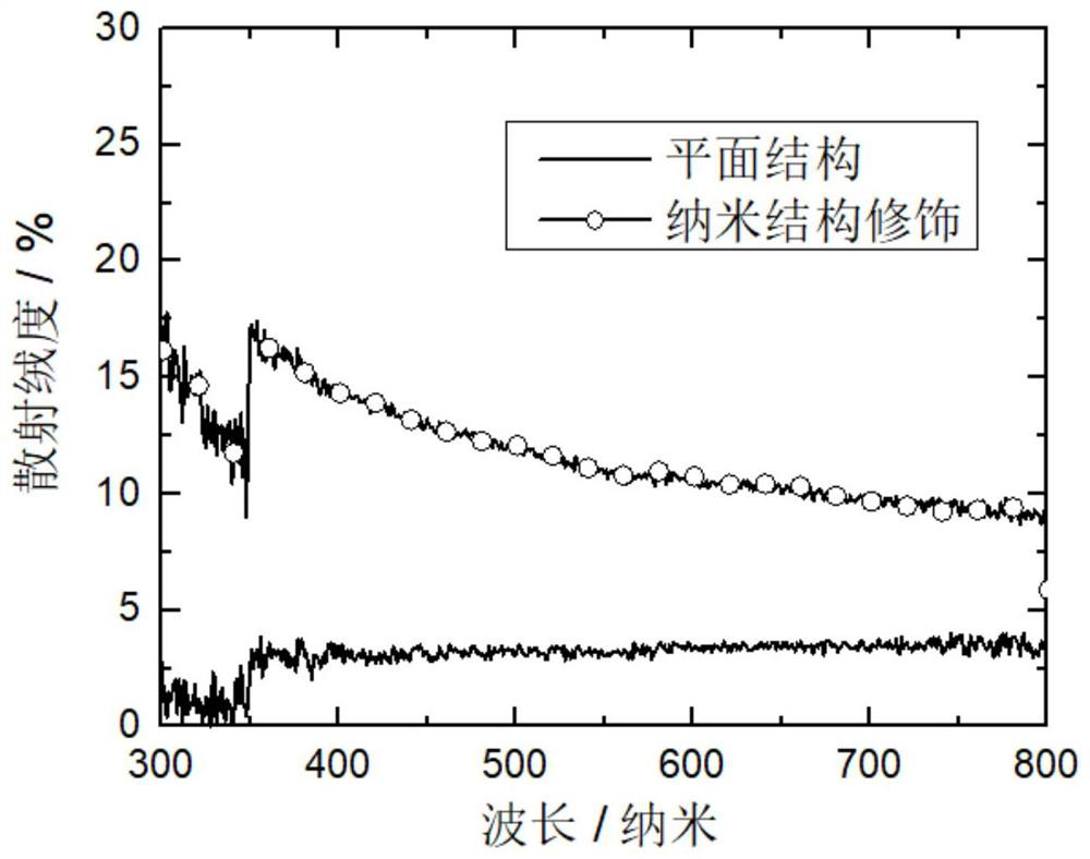
Nanostructure-modified electron transport layer
An electron transport layer, nanostructure technology, applied in circuits, electrical components, electrical solid devices, etc., can solve problems such as light absorption loss
- Summary
- Abstract
- Description
- Claims
- Application Information
AI Technical Summary
Problems solved by technology
Method used
Image

Examples
Embodiment 1
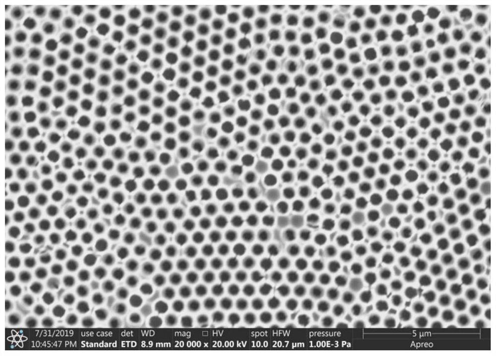
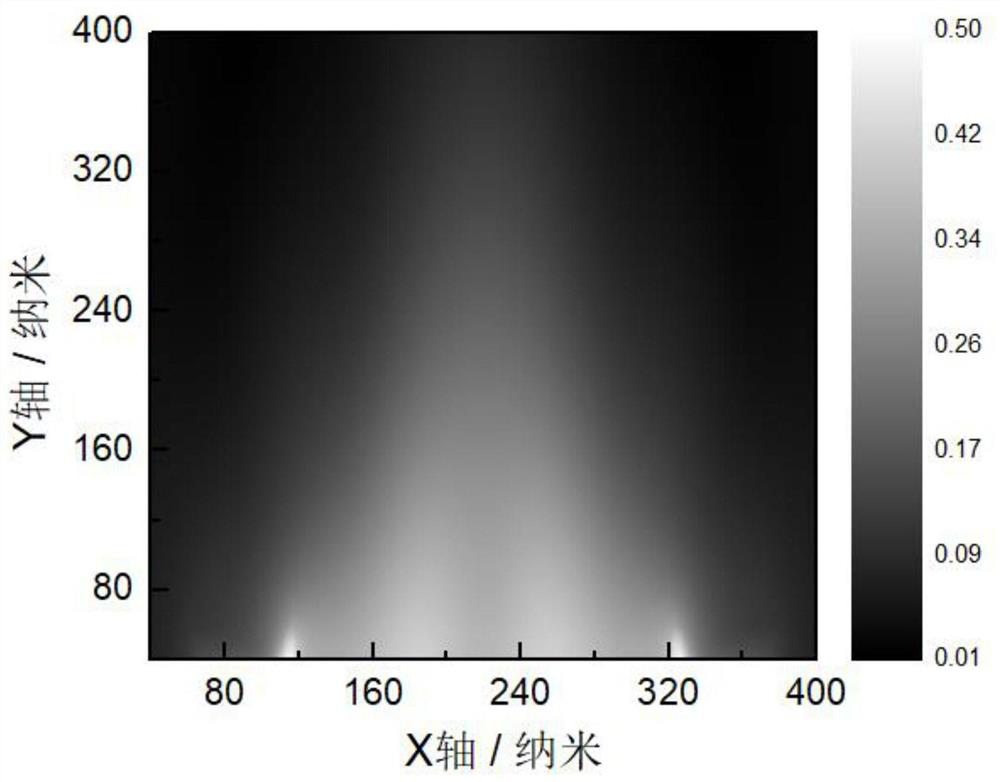
[0024] A nanostructure-modified electron transport layer, the structure of which is as follows:
[0025] 1) Add 1ml tin dioxide (SnO 2 ) Nanoparticle stock solution and 3ml deionized water were mixed in a ratio of 1:3, and 600 μl of monodisperse polystyrene (PS) nanosphere latex solution with a particle size of 2.5wt% and a particle size of 700mn was taken, and it was mixed evenly by ultrasonication for 10min , the prepared SnO 2 The aqueous solution is mixed with the PS nanosphere latex solution and stirred evenly.
[0026] 2) Ozone treatment is performed on the ITO transparent electrode to increase the hydrophilicity of the surface and the removal of organic matter, take 100 μl PS nanospheres and SnO 2 The mixed aqueous solution was drip-coated on the surface of the ozone-treated ITO, and the spin-coating process was used to make it evenly distributed. The spin-coating speed of the homogenizer was set at 3000rpm, and the spin-coating time was set at 30s; then the annealing...
Embodiment 2
[0031] A nanostructure-modified electron transport layer, the structure of which is as follows:
[0032]1) Mix 1ml of zinc oxide (ZnO) nanoparticle stock solution and 3ml of deionized water at a ratio of 1:3, and take 600 μl of monodisperse polystyrene (PS) nanosphere latex with a particle size of 1.5wt% and a particle size of 300mn solution, ultrasonic 10min to make it evenly mixed, and the prepared ZnO aqueous solution and PS nanosphere latex solution were mixed and stirred evenly.
[0033] 2) Ozone treatment is performed on the ITO transparent electrode to increase the hydrophilicity of its surface and the removal of organic matter. Take 100 μl of PS nanospheres and ZnO mixed aqueous solution and drop-coat it on the ozone-treated ITO surface, and use a spin-coating process to make it evenly distributed. The spin-coating speed of the homogenizer was set at 1500rpm, and the spin-coating time was set at 50s; then an annealing process was used to achieve a good grain boundary o...
PUM
| Property | Measurement | Unit |
|---|---|---|
| Thickness | aaaaa | aaaaa |
| Particle size | aaaaa | aaaaa |
Abstract
Description
Claims
Application Information