Beam splitting/combining waveguide based on GOI or SOI and preparation method thereof

A beam-splitting technology, applied in the field of semiconductor optoelectronics, can solve the problems of difficult preparation, complex beam-splitting/beam-combining waveguide processes, etc., achieving uncomplicated processes, strong light distribution and synthesis capabilities, and large-scale silicon photonics integration. Effect

Pending Publication Date: 2021-04-02
HAINAN NORMAL UNIV
View PDF16 Cites 0 Cited by
  • Summary
  • Abstract
  • Description
  • Claims
  • Application Information

AI Technical Summary

Problems solved by technology

[0004] In view of this, the present invention provides a beam-splitting / combining waveguide structure based on GOI or SOI materials and a preparation method thereof, which effectively solves the problem of complicated beam-splitting / combining waveguides in the prior art and difficulty in preparation. question

Method used


Image

  • Beam splitting/combining waveguide based on GOI or SOI and preparation method thereof
  • Beam splitting/combining waveguide based on GOI or SOI and preparation method thereof
  • Beam splitting/combining waveguide based on GOI or SOI and preparation method thereof

Examples


preparation example Construction

[0049] A method for preparing a beam splitting / combining waveguide structure based on GOI or SOI, comprising the following steps:

[0050] (1) Prepare a beam splitting / combining waveguide structure pattern with photoresist on the intrinsic single crystal Ge layer or intrinsic single crystal Si layer of the GOI or SOI epitaxial wafer through the photolithography process of the negative version of the positive resist;

[0051] (2) Deposit 100-400nm Al on GOI or SOI epitaxial wafers with photoresist waveguide patterns by magnetron sputtering or physical vapor deposition at a temperature less than 150° 2 o 3 or SiO 2 Floor;

[0052] (3) will have SiO 2 The epitaxial wafer of the first layer is soaked in acetone for 5-60 minutes, and then repeatedly passed ultrasonication in acetone for 5-30 minutes until the photoresist and the Al on it are removed. 2 o 3 or SiO 2 up to the layer;

[0053] (4) After cleaning with absolute ethanol, blow dry the surface of the waveguide patte...

Embodiment 1

[0057] In this embodiment, an N-type single crystal Si substrate is taken as an example:

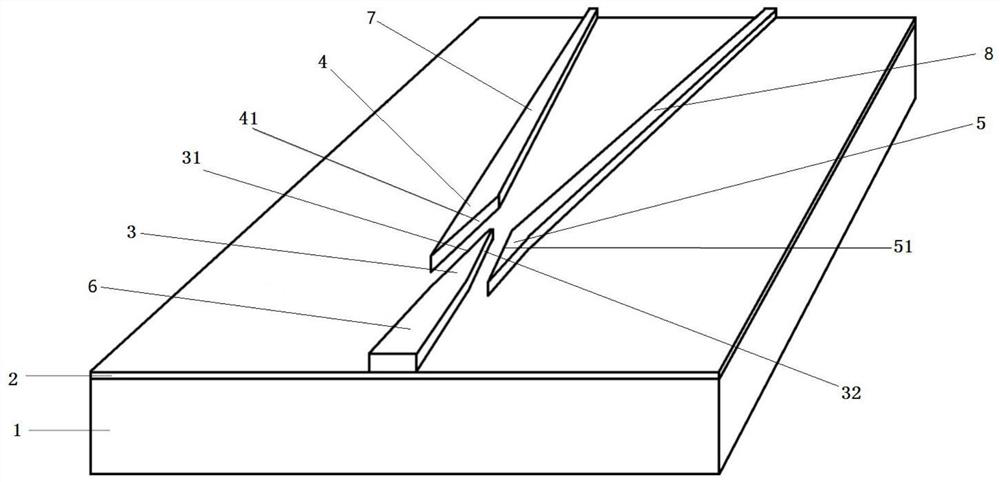
[0058] An SOI-based beam splitting / combining waveguide structure includes: doping concentration 3E18cm -3 , N-type single crystal Si substrate 1 with a thickness of 460 μm; SiO grown on the upper surface of the substrate 2 Insulating dielectric film 2; in SiO 2 An intrinsic single crystal Si layer with a thickness of 300nm is grown on the surface of the insulating dielectric film; on the intrinsic crystal layer, a waveguide pattern with a photoresist with a thickness of 1.4 μm is realized through a photolithography process of a negative version of the photoresist; through magnetron sputtering Deposit 100nm SiO on the SOI epitaxial wafer with photoresist waveguide pattern by physical vapor deposition at a temperature of less than 150° 2 layer; by incorporating SiO 2 The epitaxial wafer of the first layer was soaked in acetone for 30 minutes, and then repeatedly passed ultrasonication i...

Embodiment 2

[0060] In this embodiment, an N-type single crystal Ge substrate is taken as an example:

[0061] A GOI-based beam splitting / combining waveguide structure: including an N-type single crystal Ge substrate 1 with a doping concentration of 3E18cm-3 and a thickness of 460 μm; SiO grown on the upper surface of the substrate 2 Insulating dielectric film 2; in SiO 2 An intrinsic single crystal Ge layer with a thickness of 200nm is grown on the surface of the insulating dielectric film; on the intrinsic crystal layer, the waveguide pattern with a 1.4μm thick photoresist is realized through the photolithography process of the negative plate; through the magnetron sputtering Deposit 100nm SiO2 on GOI epitaxial wafers with photoresist waveguide patterns by physical vapor deposition at temperatures less than 150° 2 layer; by incorporating SiO 2 The epitaxial wafer of the first layer was soaked in acetone for 30 minutes, and then repeatedly passed ultrasonication in acetone for 15 minute...


PUM

PropertyMeasurementUnit
thicknessaaaaaaaaaa
thicknessaaaaaaaaaa
lengthaaaaaaaaaa

Abstract

The invention discloses a beam splitting/combining waveguide structure based on GOI or SOI. The beam splitting/combining waveguide structure comprises a substrate, an insulating medium low-refractive-index layer and a beam splitting/combining waveguide; wherein the beam splitting/combining waveguide and the insulating medium low-refractive-index layer are sequentially prepared on the upper surfaceof the substrate from top to bottom; the beam splitting/combining waveguide comprises a single-path conical waveguide, a double-path wedge-shaped waveguide and a connecting waveguide; the single-pathconical waveguide is arranged between the left wedge-shaped waveguide and the right wedge-shaped waveguide; the invention further discloses a preparation method of the waveguide structure for the GOIor SOI-based beam splitting/combining waveguide structure. According to the structure, the GOI or SOI beam splitting/combining waveguide has the determined optical power beam splitting and combiningcapacity, and the GOI or SOI beam splitting/combining waveguide has the advantages of low cost, high light splitting efficiency, high mode field light precision and high integration degree.

Description

technical field [0001] The invention relates to the technical field of semiconductor optoelectronics, and more specifically relates to a beam splitting / combining waveguide structure based on GOI or SOI materials and a preparation method thereof. Background technique [0002] Silicon photonics devices can meet the data center's reliance on lower cost, higher integration, more embedded functions, higher interconnect density, lower power consumption and reliability. [0003] At present, the light source beam splitting / combining waveguides of traditional silicon photonics integrated chips have a series of problems such as high design accuracy requirements, complex process, difficult preparation, high cost, low integration, and difficulty in realizing high-precision distribution of light sources. Therefore, how to develop a waveguide based on GOI or SOI with simple process, low cost, high integration, and easy to realize high-precision distribution and beam splitting / combining of...

Claims


Application Information

Patent Timeline
Patent Type & Authority Applications(China)
IPC IPC(8): G02B6/122G02B6/125G02B6/136
CPCG02B6/1228G02B6/125G02B6/136G02B2006/1215G02B2006/12147
Inventor 乔忠良赵志斌李再金陈浩刘国军李林曲轶
Owner HAINAN NORMAL UNIV
Why Eureka
Try Eureka