Insulating layer structure of thin film sensor based on metal substrate

A thin-film sensor, metal base layer technology, used in multilayer circuit manufacturing, cleaning/polishing of conductive patterns, printed circuits connected to non-printed electrical components, etc., can solve insulation failure, prone to pinholes, cleanliness The problem is not high, to achieve the effect of simple structure, solving short circuit, increasing time and cost

Pending Publication Date: 2021-04-02
曹建峰
View PDF0 Cites 0 Cited by
  • Summary
  • Abstract
  • Description
  • Claims
  • Application Information

AI Technical Summary

Problems solved by technology

However, conventional thin-film sensors based on silicon substrates are difficult to apply to high temperature, high pressure, large strain and corrosive situations due to the brittleness of the substrate material and the lack of high temperature resistance.
[0003] In order to solve the above problems, thin-film sensors based on metal substrates have been developed. However, due to the particularity of metal substrates, the substrates need to be polished in a traditional processing environment with low cleanliness, and then transferred to the ultra-clean room for sensor production. The substrate is very easy to contain particles and other pollutants, which will cause problems in subsequent processes
For example, aluminum oxide, an insulating material based on metal-based

Method used


Image

  • Insulating layer structure of thin film sensor based on metal substrate
  • Insulating layer structure of thin film sensor based on metal substrate

Examples


Example Embodiment

[0026] Example 1

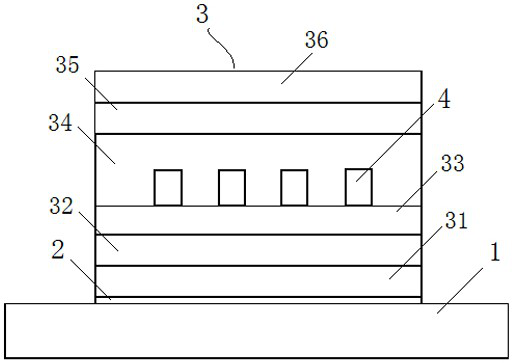
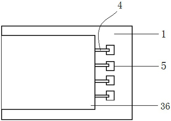
[0027] An insulating layer structure of a thin film sensor based on a metal substrate, comprising a metal substrate layer 1, an adhesive layer 2 arranged on the metal substrate layer, an insulating layer 3 arranged on the adhesive layer, and a sensor arranged on the insulating layer 3 The circuit layer 4, the insulating layer 3 is formed by layer-by-layer deposition of aluminum oxide by different processes.

Example Embodiment

[0028] Example 2

[0029] As a preferred design, the bonding layer 2 is a metal titanium layer with a thickness of 5-50 nm deposited on the metal substrate.

[0030] The insulating layer 3 is composed of three layers of aluminum oxide deposited layer by layer.

[0031] The first layer 31 of the insulating layer 3 is a layer of aluminum oxide with a thickness of 0.2-5 um deposited on the titanium metal layer by electron beam evaporation.

[0032] The second layer 32 of the insulating layer 3 is a layer of aluminum oxide with a thickness of 10-500 nm deposited on the first insulating layer 31 by atomic layer deposition.

[0033] The third layer 33 of the insulating layer 3 is a layer of aluminum oxide with a thickness of 0.2-5 um deposited on the second insulating layer 32 by electron beam evaporation.

Example Embodiment

[0034] Example 3

[0035] As a preferred design, a protective layer may also be provided on the insulating layer 3 . The first protective layer 34 is a layer of aluminum oxide with a thickness of 0.2-5 um deposited on the third insulating layer 33 by electron beam evaporation, and the first protective layer does not cover the pad 5 of the sensor circuit layer.

[0036] The function of the first protective layer 34 is to protect the circuit layer of the sensor against external damage such as scratches and abrasions, and at the same time have a certain insulation capacity.


PUM


Abstract

The invention discloses an insulating layer structure of a thin film sensor based on a metal substrate. The structure comprises a metal substrate layer, a bonding layer arranged on the metal substratelayer, an insulating layer arranged on the bonding layer and a sensor circuit layer arranged on the insulating layer, and the insulating layer is formed by depositing aluminum oxide layer by layer atdifferent times according to different processes. According to the invention, the aluminum oxide insulating layer is rapidly manufactured by using an electron beam evaporation process, and the aluminum oxide insulating layer prepared by means of the step covering capability of an atomic layer stacking process can cover pinholes in the aluminum oxide insulating layer manufactured by using the electron beam evaporation process, so that no short circuit occurs between the sensor circuit layer and the metal substrate; and meanwhile, the thickness of the aluminum oxide insulating layer manufactured through the atomic layer stacking process is 10-500 nm, so that a large amount of time and cost cannot be generated. The structure is simple in structure, and the problem that the thin film sensor based on the metal substrate is short-circuited when used under the high-temperature environment condition is solved on the premise that time and cost are not increased.

Description

technical field [0001] The invention relates to an insulating layer structure of a thin-film sensor based on a metal substrate, belonging to the technical field of thin-film sensors. Background technique [0002] With the industrial upgrading of the industrial Internet and intelligent manufacturing, real-time monitoring of the manufacturing process has become more and more important. Not only can the acquisition of key process parameters in the manufacturing process improve product quality and improve production efficiency, but also can detect problems in advance and timely Intervene to avoid serious accidents. As a sensor that obtains key process parameters and other data, it plays a very important role. However, due to the large size of traditional sensors, it is difficult to get close to the point to be measured. Large, destroying the authenticity of detection; at the same time, due to the slow response of traditional sensors, there is a large hysteresis, it is difficult...

Claims


Application Information

Patent Timeline
IPC IPC(8): H05K3/46H05K3/00H05K3/26H05K1/18
CPCH05K1/185H05K1/186H05K3/00H05K3/0073H05K3/26H05K3/4673
Inventor 曹建峰
Owner 曹建峰
Why Eureka
Try Eureka