

Chemical palladium plating solution used in field of wafer packaging and preparation method thereof
A technology of wafer packaging and electroless plating, applied in liquid chemical plating, metal material coating process, coating, etc., can solve the problem of poor corrosion performance, ductility and bending performance, palladium plating deposition rate and dense palladium layer Uncontrollable corrosion resistance, unstable electroless palladium plating, etc., to achieve good corrosion resistance test requirements, excellent ductility, and low cost effects
- Summary
- Abstract
- Description
- Claims
- Application Information
AI Technical Summary
Problems solved by technology
Method used
Image


Examples
preparation example Construction
[0037] In order to achieve the above object, the present invention also provides a preparation method of an electroless palladium plating solution used in the field of wafer packaging, comprising the following specific steps:
[0038] 1) prepare a palladium tank, and carry a stirring pump in this palladium tank;
[0039] 2) in the palladium tank, pour into tetrahydropalladium sulfate, then add deionized water and continuously stir until the tetrahydropalladium sulfate dissolves completely, and be mixed with the mass concentration of tetrahydropalladium sulfate to obtain solution A after 25-30g / L ;
[0040] 3) successively add citric acid and malic acid whose concentration ratio is 6:1 in solution A, and obtain solution B after stirring;
[0041] 4) while continuing to stir solution B and adding the polyaminopolyether methylidene phosphonic acid that concentration is 5-15g / L, the saccharin of concentration 5-9g / L, the reducing agent that concentration is 2-5g / L, Solution C is...
Embodiment 1
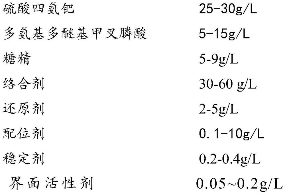
[0055]
[0056]
[0057] Among them, the bath temperature is 50°C; the time is 10min.
[0058] Using the palladium plating solution in the present embodiment, the palladium layer of the obtained plated part has a smooth and silver-white appearance; observed with a microscope, it can be clearly seen that the structure of the plated layer is very dense, the crystallization of the plated layer is meticulous and uniform, and has no cracks; after the 180° bending test, the The adhesion of the coating is very good, and no obvious cracks are observed at 100 times magnification.
Embodiment 2
[0060]
[0061] Among them, the bath temperature is 55°C; the time is 12min.
[0062] Using the palladium plating solution in the present embodiment, the palladium layer of the obtained plated part has a smooth and silver-white appearance; observed with a microscope, it can be clearly seen that the structure of the plated layer is very dense, the crystallization of the plated layer is meticulous and uniform, and has no cracks; after the 180° bending test, the The adhesion of the coating is very good, and no obvious cracks are observed at 100 times magnification.
PUM
 Abstract
Description
Claims
Application Information