
Method for measuring four-dimensional electron energy loss spectrum of to-be-measured sample

A technology of electron energy loss and sample, applied in the field of physics research, can solve the problems of momentum and energy combination, and achieve the effect of convenient upgrade

Active Publication Date: 2021-04-13
PEKING UNIV
View PDF14 Cites 0 Cited by
  • Summary
  • Abstract
  • Description
  • Claims
  • Application Information

AI Technical Summary

Problems solved by technology

[0003] However, none of these techniques combine momentum and energy, and electron energy loss spectroscopy includes rich information about the inelastic scattering of electron-atom interactions, which can deeply analyze various physical and chemical properties of substances

Method used


Image

  • Method for measuring four-dimensional electron energy loss spectrum of to-be-measured sample
  • Method for measuring four-dimensional electron energy loss spectrum of to-be-measured sample
  • Method for measuring four-dimensional electron energy loss spectrum of to-be-measured sample

Examples


Embodiment 1

[0066] This embodiment provides a method for measuring the phonon dispersion spectrum near the diamond / cubic boron nitride heterojunction interface, the method comprising the following steps:

[0067] Put the prepared diamond / cubic boron nitride heterojunction electron microscope sample into the electron microscope, adjust the belt axis, adjust the optical path at the convergence half angle of 20mrad (ie, the large convergence half angle), and switch to 3mrad convergence half angle (ie small convergence half angle) , use the projection lens to adjust the diffraction pattern, so that the central transmission spot and two first-order diffraction spots are located in the slit of the slit diaphragm, the energy channel is selected as 0.0005eV / ch, and the EELS astigmatism is adjusted, and Γ'MΓMΓ near the interface can be measured 'The dispersion signal. A monochromator can be inserted between the electron gun and the sample to limit the energy passing through the electron beam and i...

Embodiment 2

[0070] This embodiment provides a method for measuring the electronic band structure near the diamond / cubic boron nitride heterojunction interface, the method comprising the following steps:

[0071] Put the prepared diamond / cubic boron nitride heterojunction electron microscope sample into the electron microscope, adjust the belt axis, adjust the optical path at the convergence half angle of 15mrad, switch to 0.1mrad convergence half angle, and use the projection lens to adjust the diffraction pattern to make the center transmit The spot and two first-order diffraction spots are located in the slit of the slit diaphragm, the energy channel is selected as 0.01eV / ch, and the EELS astigmatism is adjusted, the electronic band structure of Γ'MΓMΓ' near the interface can be measured. A monochromator can be inserted between the electron gun and the sample to limit the energy passing through the electron beam and improve energy resolution.

Embodiment 3

[0073] This embodiment provides a method for measuring the d-d exciton dispersion relationship from the bulk state of nickel oxide NiO to the surface, the method comprising the following steps:

[0074] Put the prepared NiO electron microscope sample into the electron microscope, adjust the belt axis, adjust the optical path at the convergence half angle of 35mrad, switch to the convergence half angle of 0.5mrad, and use the projection lens to adjust the diffraction pattern so that the central transmission spot and two first-order diffraction spots Located in the slit of the slit diaphragm, the energy channel is selected to be 0.005eV / ch, the EELS astigmatism is adjusted, and the electron beam scans from the body to the surface of the sample, and the change of the dispersion of the d-d excitons of NiO from the body to the surface can be measured. A monochromator can be inserted between the electron gun and the sample to limit the energy passing through the electron beam and imp...


PUM


Abstract

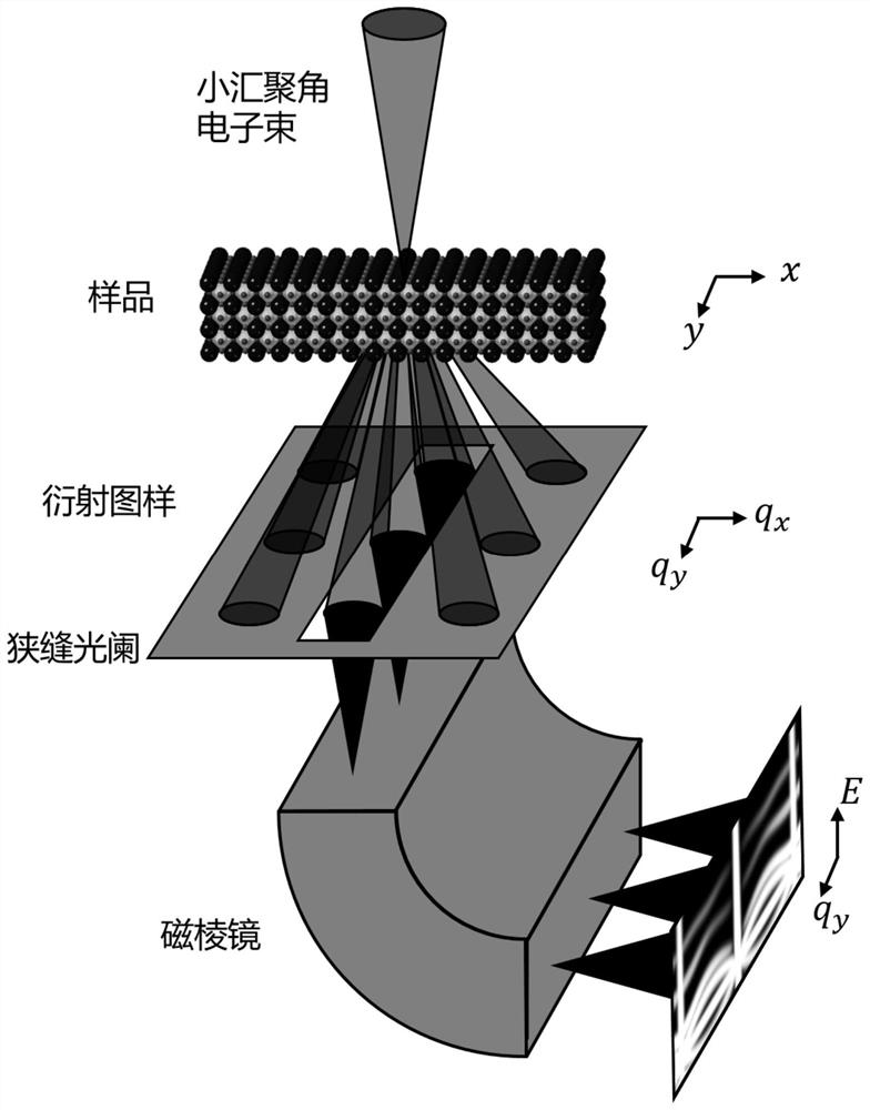
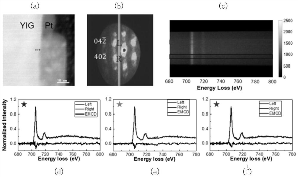
The invention provides a method for measuring a four-dimensional electron energy loss spectrum of a to-be-measured sample. The method comprises the following steps: S1, putting the prepared to-be-measured sample into an electron microscope, and rotating the to-be-measured sample to a to-be-measured band shaft; S2, correcting astigmatism when a convergence half angle of an electron beam of the electron microscope is a first convergence half angle, and then switching the convergence half angle of the electron beam to a second convergence half angle; S3, adjusting a diffraction spot on an electron microscope camera to enable a momentum area to be measured to be located in a reserved area of a slit diaphragm; S4, inserting the slit diaphragm to enable the slit diaphragm to be located in the reserved area; S5, inserting a monochromator, limiting the energy passing through the electron beam, and improving an energy resolution; S6, adjusting the astigmatism; and S7, obtaining an energy-momentum diagram of the current position of the to-be-measured sample. The method can be used for measuring the energy-momentum spectrum of a nanostructure, does not need a large single crystal sample, and is an effective supplement for an angle resolution photoelectron spectroscopy and a high resolution electron energy loss spectrometer.

Description

technical field [0001] The invention realizes the measurement of the four-dimensional electron energy loss spectrum (two-dimensional space + energy + momentum) by using the novel slit aperture, can characterize the electrical and magnetic properties of materials, and is applied to physics research. Background technique [0002] In recent years, with the development of electron microscopy, ordinary imaging methods such as annular dark field images and central bright field images have become more and more limited because they can only obtain intensity information. Scientists have proposed a variety of methods to obtain more dimensional information, such as stacked diffraction imaging technology: the incident beam is scanned on the sample, and the two-dimensional diffraction intensity pattern is recorded at each scanning position, thereby constructing a four-dimensional diffraction Data; Ultrafast Transmission Electron Microscopy: This technology combines the spatial resolution...

Claims


Application Information

Patent Timeline
Patent Type & Authority Applications(China)
IPC IPC(8): G01N23/20058
CPCG01N23/20058G01N2223/0565G01N2223/102
Inventor 高鹏李跃辉时若晨
Owner PEKING UNIV
Learn More