Method for activating CdTe thin film solar cell
A thin-film solar cell and activation method technology, applied in circuits, electrical components, photovoltaic power generation, etc., can solve the problems of complicated and lengthy processes, poor compatibility, etc., and achieve the effect of promoting lattice growth and preventing oxidation.
- Summary
- Abstract
- Description
- Claims
- Application Information
AI Technical Summary
Problems solved by technology
Method used
Image
Examples
Embodiment 1
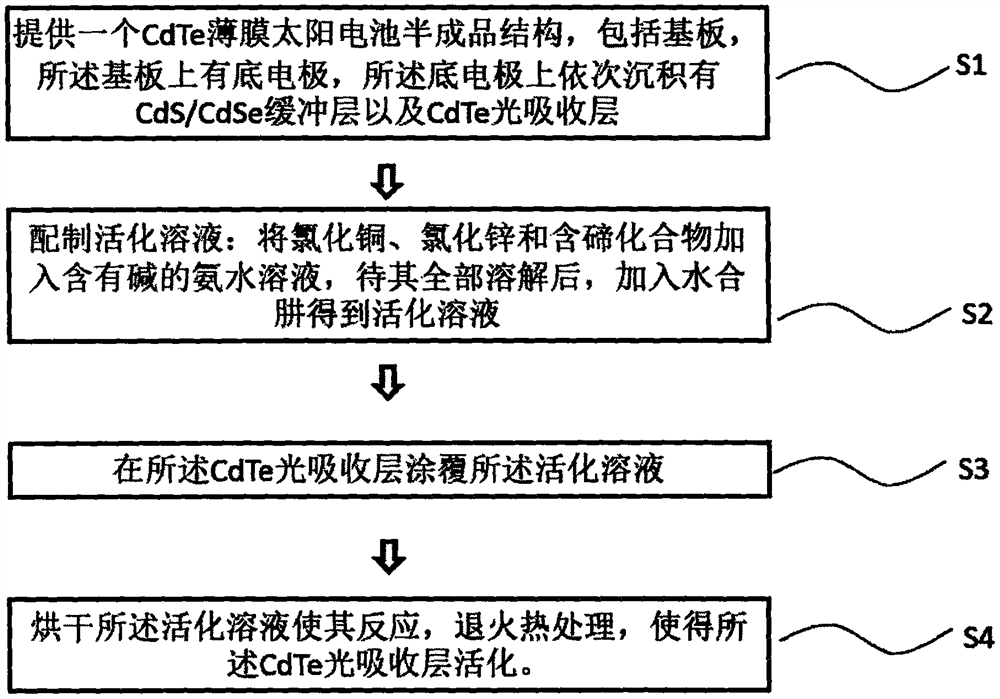
[0041] A CdTe thin film solar cell semi-finished structure is provided, including a substrate 100, a bottom electrode 200 is arranged on the substrate 100, a CdS / CdSe buffer layer 301 and a CdTe light absorption layer 302 are sequentially deposited on the bottom electrode 200; the substrate 100 is a tempered glass substrate, organic glass One of the substrates; the bottom electrode 200 is an ITO conductive film layer. The CdS / CdSe buffer layer 301 has a thickness of 10 nm, and the CdTe light absorbing layer 302 has a thickness of 2.0 μm.
[0042] Prepare activation solution 500, add cupric chloride, zinc chloride and tellurium oxide to ammonia solution containing sodium hydroxide, after all of them dissolve, add hydrazine hydrate to obtain activation solution, pH value 12.5, zinc element content 0.05mol / L, Copper element 0.01mol / L, tellurium element 0.06mol / L, hydrazine hydrate 0.4mol / L.
[0043] The activation solution 500 is spin-coated on the CdTe light absorbing layer 302...
Embodiment 2
[0047] A CdTe thin film solar cell semi-finished structure is provided, including a substrate 100, a bottom electrode 200 is arranged on the substrate 100, a CdS / CdSe buffer layer 301 and a CdTe light absorption layer 302 are sequentially deposited on the bottom electrode 200; the substrate 100 is a tempered glass substrate, organic glass One of the substrates; the bottom electrode 200 is an ITO conductive film layer. The CdS / CdSe buffer layer 301 has a thickness of 150 nm, and the CdTe light absorbing layer 302 has a thickness of 10 μm.
[0048] Prepare the activation solution 500, add copper chloride, zinc chloride and potassium tellurite to the ammonia solution containing potassium hydroxide, after all of them dissolve, add hydrazine hydrate to obtain the activation solution, the pH value is 14, and the zinc element content is 0.15mol / L, copper element 0.015mol / L, tellurium element 0.15mol / L, hydrazine hydrate 0.8mol / L.
[0049] The activation solution 500 is spin-coated ...
Embodiment 3
[0053] A CdTe thin film battery semi-finished structure is provided, including a substrate 100, a bottom electrode 200 is arranged on the substrate 100, a 40nm MgZnO window layer 400, a CdS / CdSe buffer layer 301 and a CdTe light absorption layer 302 are sequentially deposited on the bottom electrode 200; the substrate 100 is One of tempered glass substrate and plexiglass substrate; the bottom electrode 200 is an ITO conductive film layer. The CdS / CdSe buffer layer 301 has a thickness of 50 nm, and the CdTe light absorbing layer 302 has a thickness of 2.0 μm.
[0054] Prepare the activation solution 500, add copper chloride, zinc chloride and sodium tellurite to the ammonia solution containing sodium hydroxide, after it is completely dissolved, add hydrazine hydrate to obtain the activation solution, the pH value is 13, and the zinc element content is 0.1mol / L, copper element 0.02mol / L, tellurium element 0.115mol / L, hydrazine hydrate 0.5mol / L.
[0055] The activation solution...
PUM
| Property | Measurement | Unit |
|---|---|---|
| Thickness | aaaaa | aaaaa |
| Thickness | aaaaa | aaaaa |
| Thickness | aaaaa | aaaaa |
Abstract
Description
Claims
Application Information


