

Structural color functional nanostructure and preparation method thereof
A functional nano and structural color technology, applied in the field of structural color, can solve problems such as the limited purity of structural color pixels, and achieve the effect of high resolution and high purity
- Summary
- Abstract
- Description
- Claims
- Application Information
AI Technical Summary
Problems solved by technology
Method used
Image

Examples
preparation example Construction
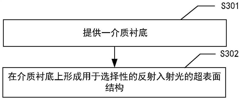
[0064] According to an embodiment of the present invention, the deposition method of the above preparation method includes at least one of the following: ion beam sputtering, magnetron sputtering, electron beam evaporation, atomic layer deposition, and self-oxidation.
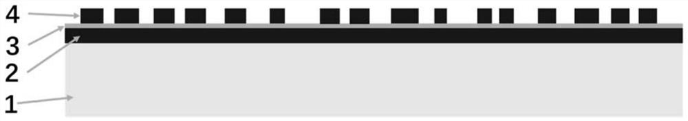
[0065] According to an embodiment of the present invention, a metal film, an ultra-thin dielectric layer, and an array of metal nanoparticles are formed on a dielectric substrate through a standard semiconductor process, thereby preparing a structurally colored functional nanostructure based on an ultra-thin dielectric layer, which is small in size and Easy to integrate. Compared with dielectric nanostructures, ultra-thin dielectric layers have unique scattering properties due to the formation of waveguide modes. Therefore, the structural color functional metasurface structure based on the ultra-thin dielectric layer has the advantages of high resolution and low loss.
[0066] According to the embodiments of t...
Embodiment 1
[0068] In this embodiment, the material of the dielectric substrate is a silicon substrate, the material of the metal film is silver, the material of the ultra-thin dielectric layer is silicon oxide, and the material of the metal nanoparticles is aluminum. The preparation method is as follows:
[0069] cleaning silicon substrates;
[0070] A metal silver film with a thickness of 120nm is deposited and grown on a silicon substrate by a magnetron sputtering process;
[0071] Deposit and grow an ultra-thin dielectric layer of silicon oxide with a thickness of 5nm on the metal silver film by magnetron sputtering process;
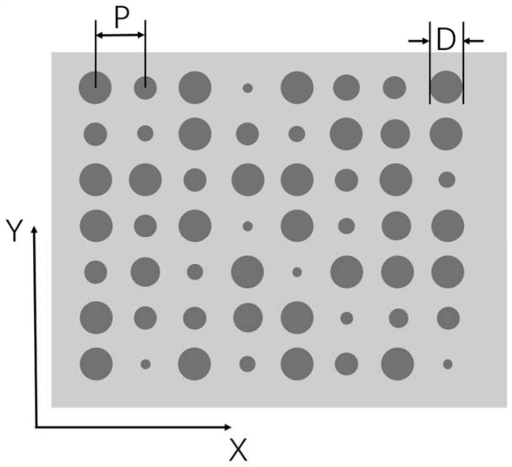
[0072] Spin-coat PMMA electron beam photoresist with a thickness of 150nm on the surface of ultra-thin dielectric layer silicon oxide, and form a circular hole array on the PMMA electron beam photoresist by electron beam lithography technology, the array period is 280nm, and the diameter of the circular hole is 60 ~200nm; through the method of electron beam eva...
Embodiment 2
[0075] In this embodiment, the material of the dielectric substrate is a silicon dioxide substrate, the material of the metal film is aluminum, the material of the ultra-thin dielectric layer is aluminum oxide, and the material of the metal nanoparticles is aluminum. The preparation method is as follows:
[0076] cleaning the silica substrate;
[0077] A metal aluminum film with a thickness of 100nm is evaporated on a silicon dioxide substrate by electron beam;
[0078] Place the metal aluminum film in the air to self-oxidize to form an ultra-thin dielectric layer of aluminum oxide with a thickness of 3nm;
[0079] Spin-coat PMMA electron beam photoresist with a thickness of 150nm on the surface of ultra-thin dielectric layer alumina, and form a square hole array on the PMMA electron beam photoresist by electron beam lithography technology, the array period is 200nm, and the side length of the square hole 130nm; through the method of electron beam evaporation, metal aluminum ...
PUM
| Property | Measurement | Unit |
|---|---|---|
| Thickness | aaaaa | aaaaa |
| Thickness | aaaaa | aaaaa |
| Diameter | aaaaa | aaaaa |
Abstract
Description
Claims
Application Information