Method for patterning transfer of graphdiyne film
A graphdiyne and patterning technology, applied in the field of patterned transfer graphdiyne thin films, can solve the problems of difficulty in etching clean by patterned etching, limiting the application of graphdiyne characterization and analysis, uncontrollable shape and area of graphdiyne thin films, etc. The effect of increasing the complexity of the process
- Summary
- Abstract
- Description
- Claims
- Application Information
AI Technical Summary
Problems solved by technology
Method used
Image
Examples
Embodiment 1
[0042] 1. Uniform photoresist on Si substrate with 300nm thick oxide layer - pre-baking - UV exposure - post-baking - development - thermal evaporation of chromium gold - deglue - get a pattern with 400 field electrodes The mark is the target base.
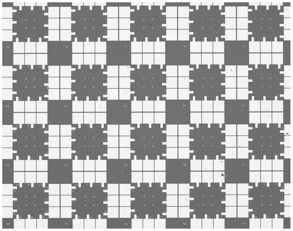
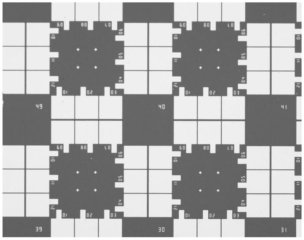
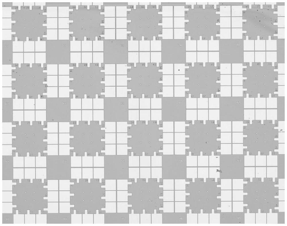
[0043] 2. Cut the target substrate into small pieces of 5mm×5mm (such as Figure 1a and Figure 1b Shown), uniform polymethyl methacrylate (such as Figure 2a and Figure 2b shown), and then carry out patterned electron beam exposure to polymethyl methacrylate (each field exposes a square pattern with a size of 70 μm×70 μm), develop, and expose the place where the graphyne film pattern is expected to be transferred (such as Figure 3a and Figure 3b shown).
[0044] 3. Thin the graphyne on the copper foil to 10-20nm by oxygen plasma reaction etching, evenly spread polymethyl methacrylate on the copper foil with graphyne film, heat and dry at 120°C / 1min The copper foil was removed by etching with a saturated ferric chloride so...
Embodiment 2
[0047] 1. Uniform photoresist on the Si substrate with a 300nm thick oxide layer - pre-baking - ultraviolet exposure - post-baking - development - thermal evaporation of chromium gold - deglue - to obtain a 400-field electrode pattern The mark is the target base.
[0048] 2. Cut the target substrate into large pieces of 3cm×3cm, apply the photoresist evenly, and dry it before 85℃ / 2min, then pattern the photoresist with UV exposure, and then heat it at 95℃ / 80s and then dry it. Develop to expose the place where the graphyne film pattern is expected to be transferred.
[0049] 3. Thin the graphdiyne (2.5×2.5cm) on the copper foil to 10-20nm by reactive etching with oxygen plasma, evenly spread polymethyl methacrylate on the copper foil with the graphdiyne film twice, Heat and dry at 120°C / 1min, and use saturated ferric chloride solution to react for 12h to etch and remove the copper foil. Use a clean silicon wafer to pick up the polymethyl methacrylate with graphyne attached, a...
PUM
| Property | Measurement | Unit |
|---|---|---|
| thickness | aaaaa | aaaaa |
Abstract
Description
Claims
Application Information


