Preparation method of medium-voltage shield gate field effect transistor

A technology of field-effect transistors and shielding gates, which is applied in semiconductor/solid-state device manufacturing, semiconductor devices, electrical components, etc., can solve the problems of high process cost, shortened channel length, and high matching requirements, so as to reduce process cost and difficulty, prevent thick oxygen step difference, and ensure the effect of etching quality

Pending Publication Date: 2021-05-28
上海恒灼科技有限公司
View PDF4 Cites 2 Cited by
  • Summary
  • Abstract
  • Description
  • Claims
  • Application Information

AI Technical Summary

Problems solved by technology

After the polysilicon is filled in the trench, chemical mechanical polishing (CMP) is used to polish off the polysilicon and thick oxygen in the active area to eliminate the thick oxygen step in the above-mentioned transition area, and leave residues after the control gate polysilicon is etched in the subsequent process. Leakage between gate and source, this method requires polysilicon grinding equipment, and the process cost is high
If polysilicon is etched by low-cost dry etching method without using CMP equipment, due to the high selectivity ratio of etching to polysilicon and the underlying silicon dioxide, silicon dioxide will not be etched basically. The thick silicon dioxide on the active area will be removed by wet etching after definition by photolithography, but the thick silicon dioxide in the range of the terminal guard ring and the source polysilicon that is at the same potential as the active area cannot be removed, so in the same way as Thick oxygen steps will be formed in the transition region of the original cell. To eliminate the problem of control gate polysilicon residue, more excessive etching is required, which will cause the thickness of the control gate polysilicon in the trench of the original cell area to be very thin, and the metal connection via hole of the control gate It is easy to cut through and destroy the silicon dioxide isolation layer between the shield gate (connected to the source) and the control gate, which brings the same risk of gate-source leakage. In addition, excessive etching of the control gate will also cause channel The length becomes shorter, causing large threshold voltage fluctuations
This kind of process requires a high degree of matching with the device layout design, and the process control is difficult

Method used


Image

  • Preparation method of medium-voltage shield gate field effect transistor
  • Preparation method of medium-voltage shield gate field effect transistor
  • Preparation method of medium-voltage shield gate field effect transistor

Examples


Embodiment Construction

[0037]In order to make the objects, technical solutions, and advantages of the present invention, the technical solutions of the present invention will be further explained below.

[0038]The present invention proposes a method of preparing a medium pressure shield gate effect transistor, comprising the steps of:

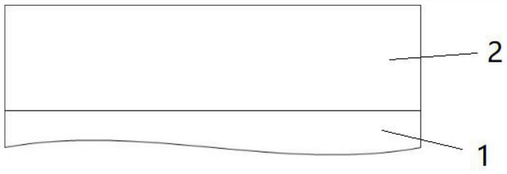
[0039]Step 1: Prepare the substrate;figure 1 As shown, the bottom layer is an N-type arsenic strain substrate 1, a resistivity range: 1mohm.cm ~ 3mohm.cm, located on the bottom surface of N-arsenic epitaxial layer 2, resistivity range: 150mohm.cm ~ 400mohm.cm , Thickness: 5 um ~ 10um.

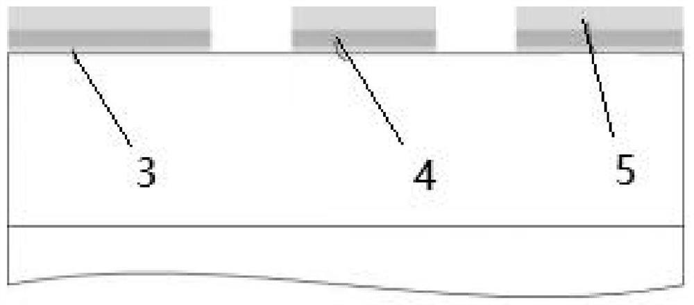
[0040]Step 2: The first layer of silica layer 3 is generated in the active region and the terminal region of the substrate surface and the terminal region, the first layer of silica layer 3 thickness is 500 angstroms ~ 1000 angstroms; preventing the trench 8 thick field oxygen 6 The thick silica is also grown in an active region during the growth process.

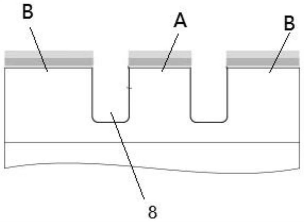
[0041]Step 3: A layer of silicon nitride lay...


PUM

PropertyMeasurementUnit
thicknessaaaaaaaaaa
thicknessaaaaaaaaaa
thicknessaaaaaaaaaa

Abstract

The invention provides a preparation method of a medium-voltage shield gate field effect transistor, which adopts silicon dioxide (SiO2)/silicon nitride (SiN)/silicon dioxide (SiO2) (ONO structure for short) as a trench barrier layer (ONOHardmask for short), prevents a thick oxygen step difference from being generated in a transition region on the surface of a substrate, and eliminates the hidden danger of electric leakage between a gate electrode and a source electrode.

Description

Technical field[0001]The present invention relates to the field of transistors, and more particularly to a method of preparing a medium pressure shield gate effect transistor.Background technique[0002]Medium pressure shield gate effect transistor (SGT) trench inverse oxygen thickness generally requires 3000 angstroms (the higher the device withstand voltage requirements, the field oxygen), the corresponding scheme needs to be selected during the manufacturing process to prevent the formation protection ring The paralysis difference between the transition area is too high, resulting in control of the control gate polysilicon residue. At present, the groove etch barrier layer in the medium pressure SGT manufacturing process mainly uses silica. After the trench is etched, the thick field oxygen mentioned above after the layer of silica is removed after the groove is etched. Outside the sidewall and bottom, the active region (Active) silicon surface also produces silica similar to thick...

Claims


Application Information

Patent Timeline
Patent Type & Authority Applications(China)
IPC IPC(8): H01L29/423H01L29/78H01L21/336
CPCH01L29/4236H01L29/7813H01L29/66734
Inventor 蔡斌君
Owner 上海恒灼科技有限公司
Why Eureka
Try Eureka