1S1R device based on metallic insertion layer and preparation method thereof
A 1S1R, metallic technology, applied in the field of information storage, can solve the problems of insufficient anti-crosstalk ability, insufficient leakage current suppression performance, low stability, etc., and achieve the effects of stable electrical performance, enhanced stability, and stable performance.
- Summary
- Abstract
- Description
- Claims
- Application Information
AI Technical Summary
Problems solved by technology
Method used
Image

Examples
preparation example Construction
[0062] Based on the same inventive concept, the present application also provides a method for preparing a 1S1R device based on metallic intercalation, comprising the following steps:
[0063] S1, providing the bottom electrode;
[0064] S2, preparing a conversion layer on the surface of the bottom electrode;
[0065] S3. Prepare a metallic intercalation layer on the surface of the conversion layer away from the bottom electrode;
[0066] S4. Prepare a resistive switch layer on the surface of the metal intercalation layer away from the bottom electrode;
[0067] S5. Prepare a top electrode on the surface of the resistive layer away from the bottom electrode;
[0068] Wherein, the metal intercalation material is one of Ti thin film, ITO thin film and TiN thin film.
[0069] The preparation method of the metallic intercalation layer in S3 is as follows: install titanium, indium tin oxide or titanium nitride on the magnetron sputtering equipment as the target material, control...
Embodiment 1
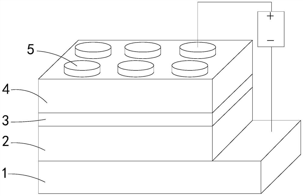
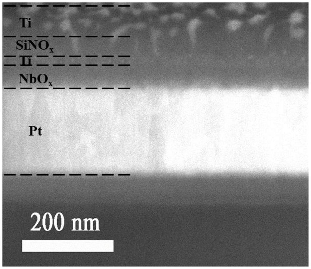
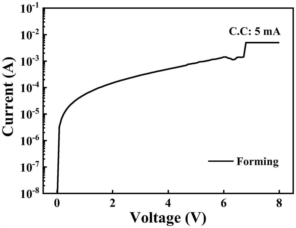
[0075] This embodiment provides a 1S1R device based on metallic intercalation, including a bottom electrode 1, a conversion layer 2, a metallic intercalation layer 3, a resistive layer 4, and a top electrode 5; wherein, the material of the bottom electrode 1 is Pt, The thickness is about 200nm; the material of conversion layer 2 is niobium oxide (NbO x ) film with a thickness of about 47nm; the material of the metallic intercalation layer 3 is a Ti film with a thickness of about 18nm; the material of the resistive layer 4 is silicon nitride (SiNO x ) film with a thickness of about 42 nm; the material of the top electrode 5 is a Ti film with a thickness of about 60 nm, and the shape of the top electrode 5 is circular with a diameter of 300 μm.
[0076] The preparation method of the above-mentioned 1S1R device is:
[0077] S1. Pretreat the surface of the carrier film substrate with the Pt bottom electrode. The pretreatment method is: sequentially use acetone, ethanol, and deion...
Embodiment 2
[0083] The structure and preparation method of the 1S1R device in this embodiment are the same as in Embodiment 1, the only difference is that in the step of preparing the resistive layer in this embodiment, the silicon dioxide target is installed on the magnetron sputtering equipment, and the other Parameters are all the same as in Example 1.
PUM
| Property | Measurement | Unit |
|---|---|---|
| Thickness | aaaaa | aaaaa |
| Thickness | aaaaa | aaaaa |
| Thickness | aaaaa | aaaaa |
Abstract
Description
Claims
Application Information
 - R&D
- Intellectual Property
- Life Sciences
- Materials
- Tech Scout
- Unparalleled Data Quality
- Higher Quality Content
- 60% Fewer Hallucinations
Browse by: Latest US Patents, China's latest patents, Technical Efficacy Thesaurus, Application Domain, Technology Topic, Popular Technical Reports.
© 2025 PatSnap. All rights reserved.Legal|Privacy policy|Modern Slavery Act Transparency Statement|Sitemap|About US| Contact US: help@patsnap.com