Field effect transistor photoelectric detector based on dielectric layer response

A technology of photodetectors and field effect tubes, applied in the field of photodetectors, can solve the problems of increasing the cost of photodetectors, small dark current, limiting device sensitivity, etc.

Active Publication Date: 2021-06-04
HUAZHONG UNIV OF SCI & TECH
View PDF14 Cites 2 Cited by
  • Summary
  • Abstract
  • Description
  • Claims
  • Application Information

AI Technical Summary

Problems solved by technology

For photoconductive photodetectors, the photoresponsive semiconductor material is also responsible for absorbing light to generate photogenerated carriers and conducting carriers; one of the difficulties involved here is that semiconductor materials with good light absorbing ability do not necessarily have good Carrier transport capability; Another difficulty is that in order to obtain high detection accuracy, the dark current caused by the defect state in the active layer semiconductor should be as small as possible, which puts forward higher requirements for semiconductor materials; Therefore, the selection and preparation of semiconductors are largely limited.
For photovoltaic photodetectors, just like the problems faced by solar cells, the recombination inside the device greatly limits the sensitivity and other performance of the device.
Although many photodetectors with excellent performance have been obtained through changes in the working environment of the device and effective control of high-quality materials in the device, these technologies have significantly increased the cost of photodetectors.

Method used


Image

  • Field effect transistor photoelectric detector based on dielectric layer response
  • Field effect transistor photoelectric detector based on dielectric layer response
  • Field effect transistor photoelectric detector based on dielectric layer response

Examples


Embodiment 1

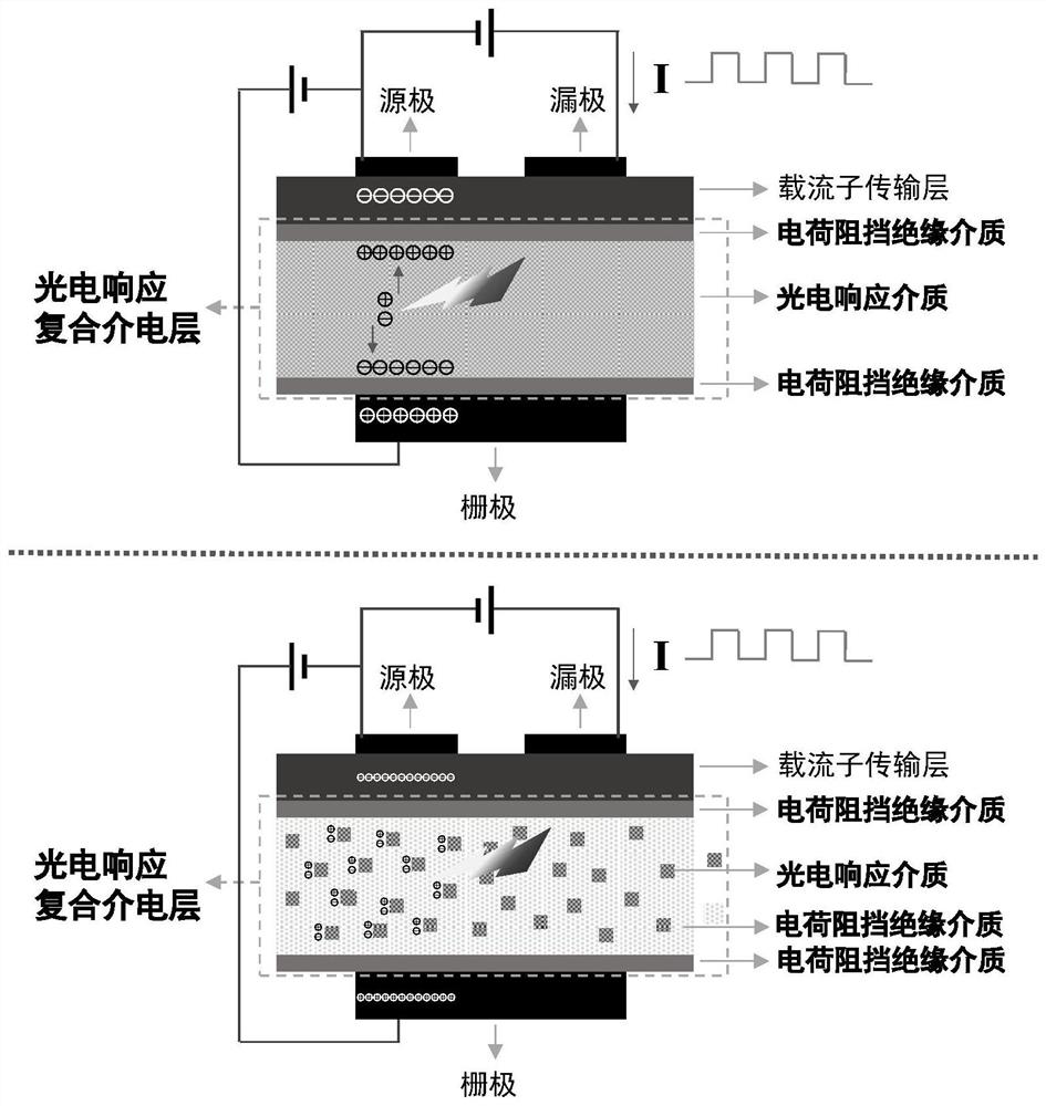
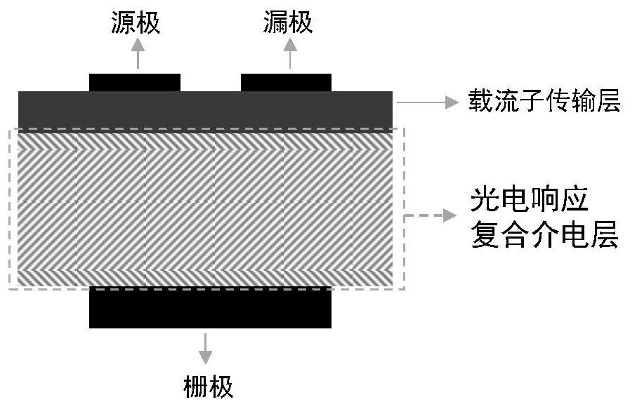
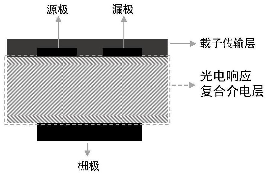
[0032] A field effect tube photodetector based on the response of a dielectric layer, such as figure 1 As shown, it includes gate, photoelectric response composite dielectric layer, carrier transport layer, source and drain; wherein, the photoelectric response composite dielectric layer is composed of photoelectric response medium and charge blocking insulating medium;

[0033] The carrier transport layer is used to transport electrons or holes, the photoresponsive medium is used to absorb light to generate electrons, holes or excitons under light, and the charge blocking insulating medium is used to confine electrons, holes, excitons, etc. The passage of electrons; the generation of photogenerated electrons, holes or excitons in the photoelectric response composite dielectric layer and their movement confined in the photoelectric response medium lead to the change of the equivalent dielectric constant of the photoelectric response composite dielectric layer, and then The chan...

example 1

[0049] Tin-doped indium oxide transparent conductive glass is used as the gate; a 20nm polymethyl methacrylate film is prepared by spin coating on it, which is used as a charge blocking insulating medium; 100nm FASnI is deposited on the polymethyl methacrylate film 3 halide perovskite layer, used as a photoelectrically responsive medium; in FASnI 3 A 10nm aluminum oxide film is deposited on the film by atomic deposition technology as a charge blocking insulating medium; a Spiro-OMeTAD film is prepared by spin coating on it as a carrier transport layer; metal source and drain are evaporated on the Spiro-OMeTAD film Pole; apply bias voltage between source, gate and drain respectively, apply 800nm ​​light to the device, test the change of current between source and drain before and after adding light, such as Figure 8 As shown, the current between the source and drain in the device changes significantly before and after the application and removal of light, and the device exhibi...

example 2

[0051] Take the aluminum oxide substrate deposited with gallium nitride, use gallium nitride as the carrier transport layer; evaporate aluminum electrodes on it as source and drain; deposit 10nm aluminum oxide on the carrier transport layer used as a charge-blocking insulating medium; then sequentially deposited 40nm of selenium as a photoresponsive medium and 10nm of aluminum oxide as a charge-blocking insulating medium, and repeated three times; subsequently, deposited an aluminum electrode as a gate; between the source and gate and the bias voltage is applied between the drains, and 500nm light is applied to the device, and the change of the current between the source and the drain before and after the light is tested, such as Figure 9 As shown, the current between the source and drain in the device changes significantly before and after the application and removal of light, and the device exhibits photoelectric response characteristics.


PUM


Abstract

The invention belongs to the field of photoelectric detectors, and particularly discloses a field effect transistor photoelectric detector based on dielectric layer response, which comprises a grid electrode, a photoelectric response composite dielectric layer, a carrier transport layer, a source electrode and a drain electrode. The composite dielectric layer is formed by compounding a photoelectric response medium and a charge blocking insulating medium; the carrier transmission layer is used for transmitting electrons or holes, the photoelectric response medium is used for absorbing light under illumination to generate electrons, holes or excitons, and the charge blocking insulating medium is used for limiting passing of the electrons, the holes and the excitons; the generation of photo-induced electrons, holes or excitons in the composite dielectric layer and the movement of the photo-induced electrons, holes or excitons limited in the photoelectric response medium cause the change of the effective dielectric constant of the composite dielectric layer and cause the change of the carrier concentration and conductivity of the carrier transport layer, and photoelectric detection is realized according to the change of the current between the source electrode and the drain electrode before and after illumination. According to the invention, the design flexibility of the photoelectric detector is obviously improved, and the photoelectric detector with high performance and low cost can be further realized.

Description

technical field [0001] The invention belongs to the field of photodetectors, and more specifically relates to a field effect tube photodetector based on the response of a dielectric layer. Background technique [0002] Optical signals contain a lot of effective information, and the effective detection of photons is helpful to obtain these information, so as to realize the collection and transmission of information. The effective detection of photons is of great significance to the development of informatization and intelligent technology. The detection technology of photons is mainly based on photodetectors, which convert optical signals into electrical signals through device design, so as to realize further processing of information. [0003] Currently, direct photodetectors are mainly based on photoconductive or photovoltaic principles. The principle of photoconductivity mainly utilizes the characteristics of the conductance change of semiconductor materials under light, ...

Claims


Application Information

Patent Timeline
Patent Type & Authority Applications(China)
IPC IPC(8): H01L31/101H01L31/0216
CPCH01L31/101H01L31/02162Y02P70/50Y02E10/549
Inventor 梅安意韩宏伟
Owner HUAZHONG UNIV OF SCI & TECH
Why Eureka
Try Eureka