Preparation method of light absorption layer and near-infrared detector, and solar cell
A light absorbing layer and detector technology, applied in the field of detectors, can solve the problems of reducing photoelectric detection efficiency, increasing dark current, and high roughness, and achieving the effects of reducing leakage current channels, improving efficiency, and reducing dark current
- Summary
- Abstract
- Description
- Claims
- Application Information
AI Technical Summary
Problems solved by technology
Method used
Image

Examples
preparation example Construction
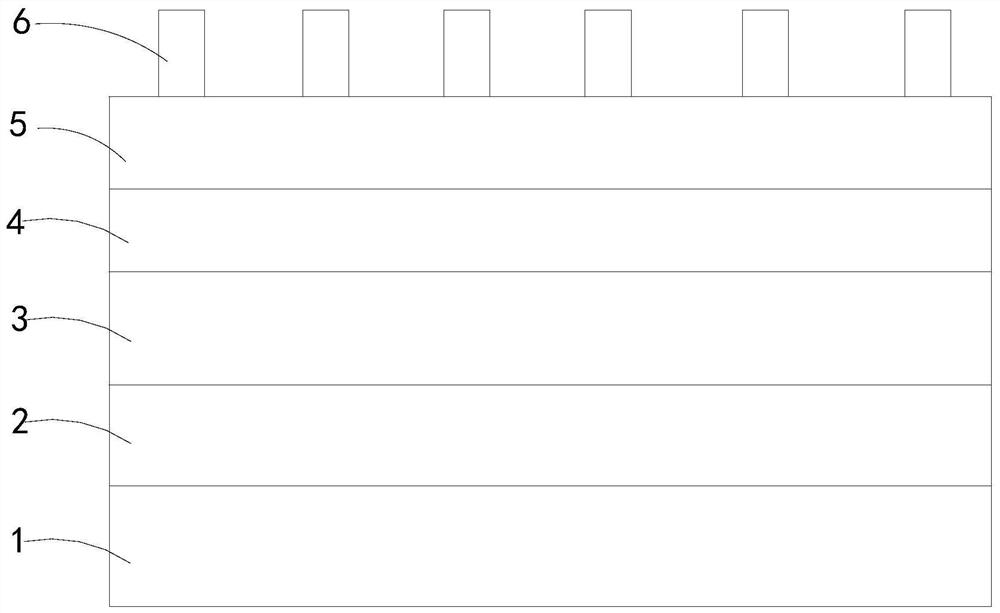
[0032] The invention provides a kind of preparation method of light absorbing layer, comprises the following steps:
[0033] S1. Provide a substrate, and prepare a bottom electrode on the substrate;
[0034] S2. Place the substrate prepared with a bottom electrode in a vacuum coating device, use Cu, Zn, Cd, Sn and Se as evaporation materials to evaporate simultaneously, and prepare a precursor on the bottom electrode;
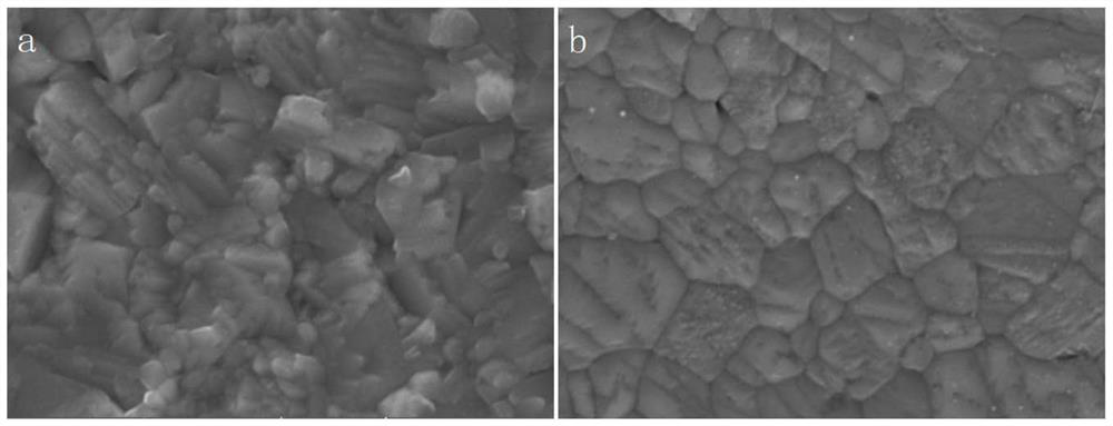
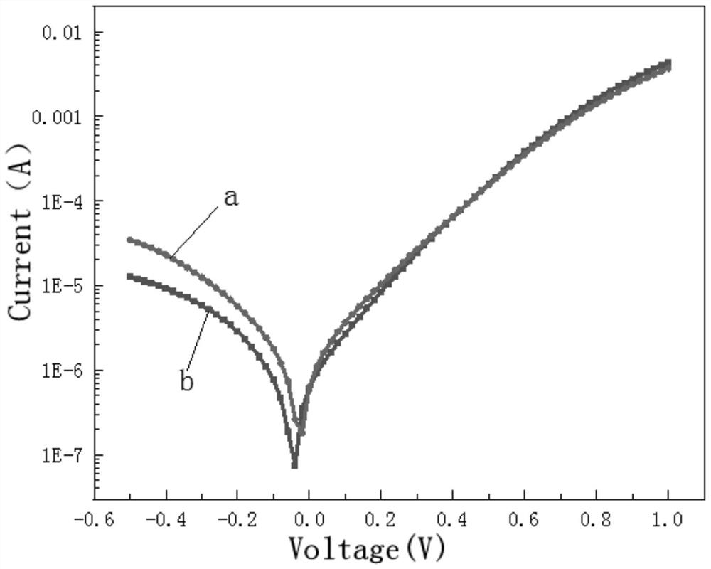
[0035] S3. Perform the first annealing on the substrate prepared with the precursor, then use the polishing solution to polish the precursor after the first annealing, then use the etching solution to etch the precursor, and finally perform the second step annealing to obtain a light absorbing layer.
[0036] It should be noted that, in the embodiment of the present application, the substrate may be one of soda lime glass, polyimide film, titanium foil, stainless steel foil, and the like.
[0037] In some embodiments, S2 is specifically: placing the substrate...
Embodiment 1
[0065] The embodiment of the present application provides a method for preparing a near-infrared detector, comprising the following steps:
[0066] A1. Provide a soda-lime glass substrate. After the substrate is cleaned, it is placed in the chamber of the magnetron sputtering equipment, with Mo as the target material, and Ar gas is introduced to control the air pressure in the chamber to be 2.0Pa. Under the power of 350W DC sputtering for 8 circles, and then control the pressure in the chamber to 0.3Pa, DC sputtering for 4 circles under 1000W power, turn off the Ar gas, take out the sample after cooling for 8min, and obtain a Mo bottom electrode with a thickness of about 500nm on the substrate surface;
[0067] A2. Place the substrate prepared with the bottom electrode into the MBE vacuum coating chamber, and control the vacuum degree of the vacuum coating chamber to be 2×10 -5 Pa, the vacuum coating equipment adopts the five-source simultaneous evaporation method, uses Cu, Zn...
PUM
| Property | Measurement | Unit |
|---|---|---|
| Particle size | aaaaa | aaaaa |
Abstract
Description
Claims
Application Information
 - Generate Ideas
- Intellectual Property
- Life Sciences
- Materials
- Tech Scout
- Unparalleled Data Quality
- Higher Quality Content
- 60% Fewer Hallucinations
Browse by: Latest US Patents, China's latest patents, Technical Efficacy Thesaurus, Application Domain, Technology Topic, Popular Technical Reports.
© 2025 PatSnap. All rights reserved.Legal|Privacy policy|Modern Slavery Act Transparency Statement|Sitemap|About US| Contact US: help@patsnap.com