Surface acoustic wave filter with discontinuous substrate structure and preparation method of surface acoustic wave filter
A surface acoustic wave, discontinuous technology, applied in piezoelectric/electrostrictive/magnetostrictive devices, electrical components, circuits, etc., to achieve the effects of low price, increased insertion loss, and increased bandwidth
- Summary
- Abstract
- Description
- Claims
- Application Information
AI Technical Summary
Problems solved by technology
Method used
Image
Examples
Embodiment 1
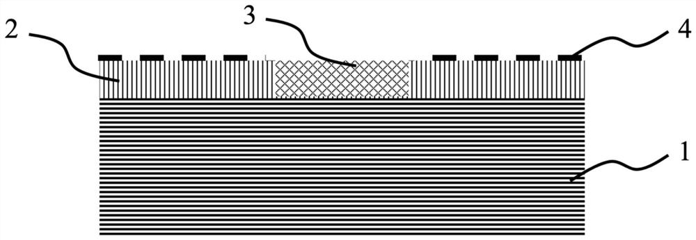
[0027] Such as figure 1 Shown is a discontinuous base structure SAW filter consisting of the following structures:
[0028] 1) substrate layer 1;
[0029] 2) The piezoelectric thin film layer 2 and the acoustic impedance discontinuous layer 3 contained therein arranged on the substrate layer;
[0030] 3) The interdigital transducer 4 arranged on the piezoelectric film layer.
[0031] As an optional embodiment, the substrate layer 1 is made of silicon, germanium, gallium arsenide, silicon carbide, sapphire, gallium nitride or aluminum nitride.
[0032] The piezoelectric thin film layer 2 is an AlN piezoelectric thin film, or an AlN piezoelectric thin film doped with one or more elements among Sc, Cr, Er, and its thickness is 100nm-10um.
[0033] The material of the acoustic impedance discontinuous layer 3 is a low-sonic material, a high-sonic material and a hollow structure, and its area is a uniform structure, a gradual structure or a periodically changing structure. In ad...
Embodiment 2
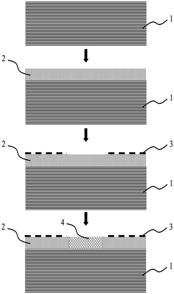
[0036] combined with figure 2 The preparation of a surface acoustic wave filter with a discontinuous base structure in this embodiment is described in detail.
[0037] 1) Prepare substrate material 1. In this embodiment, a silicon substrate is used as the substrate material. The silicon single crystal substrate used is a standard specification polished substrate, the surface is an EPI-ready polished surface cleaned by RCA, the roughness is less than 0.3nm, and the back is polished. Level, the roughness is 1±0.2μm.
[0038] 2) An AlN thin film 2 is grown on the substrate material 1 . This embodiment adopts the magnetron sputtering method (Sputter), the reaction chamber pressure is 0.3pa, the flow rate of nitrogen gas is 160sccm, the flow rate of argon gas is 40sccm, the sputtering power is 4KW, the temperature is 500°C, and the film thickness is 2um.
[0039] 3) An Al metal electrode layer 3 is fabricated on the surface of the piezoelectric film through a planar photolithog...
Embodiment 3
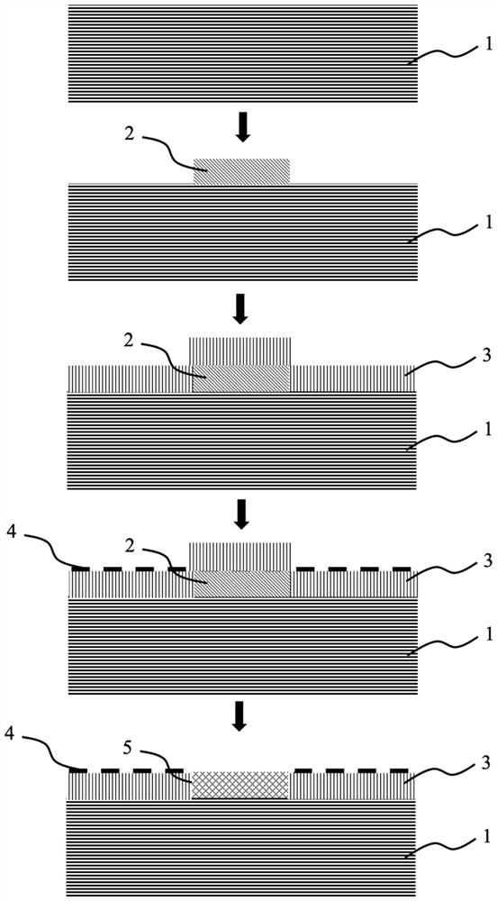
[0042] combined with image 3 The preparation of a surface acoustic wave filter with a discontinuous base structure in this embodiment is described in detail.
[0043] 1) Prepare substrate material 1. In this embodiment, a silicon substrate is used as the substrate material. The silicon single crystal substrate used is a standard specification polished substrate, the surface is an EPI-ready polished surface cleaned by RCA, the roughness is less than 0.3nm, and the back is polished. Level, the roughness is 1±0.2um.
[0044] 2) Using a negative photoresist to fabricate a structure 2 opposite to the design on the silicon (or other substrate) surface.
[0045] 3) An AlN thin film 3 is grown on the substrate material 1 . This embodiment adopts the magnetron sputtering method (Sputter), the reaction chamber pressure is 0.2pa, the flow rate of nitrogen gas is 140sccm, the flow rate of argon gas is 30sccm, the sputtering power is 3KW, the temperature is 500°C, and the film thicknes...
PUM
| Property | Measurement | Unit |
|---|---|---|
| thickness | aaaaa | aaaaa |
| thickness | aaaaa | aaaaa |
| thickness | aaaaa | aaaaa |
Abstract
Description
Claims
Application Information


