
Crystal pulling furnace for semiconductor monocrystalline silicon

A single crystal silicon and crystal pulling furnace technology, applied in the direction of single crystal growth, single crystal growth, crystal growth, etc., can solve the problems of scrap, defects, melt temperature, impurity concentration and other problems, and achieve consistency improvement , the effect of low defect density

Pending Publication Date: 2021-07-02
姜益群
View PDF0 Cites 1 Cited by
  • Summary
  • Abstract
  • Description
  • Claims
  • Application Information

AI Technical Summary

Problems solved by technology

[0002] At present, the mainstream large-diameter semiconductor crystal pulling mainly adopts the superconducting magnetic field crystal pulling technology. The strong magnetic field of 3000-8000 Gauss greatly suppresses the convection of the silicon melt in the crucible, and the stability of the melt is greatly improved. Crystal growth can be realized at an extremely low crucible rotation of about 0.5rpm, the oxygen content in silicon can be reduced to below 12ppma, and the COP of various crystal defects and vacancy defect densities is also well controlled, but the low crucible rotation brings Obvious disadvantages such as the radial fluctuation caused by the asymmetry of the thermal field, the inhomogeneity of the melt temperature and impurity concentration caused by insufficient stirring of the melt, and the detection of crystal defects will often find primary stacking faults and thermal oxidation induced stacking faults (OISF ) and other serious crystal defects, therefore, no magnetic field, oxygen content under conventional crucible rotation and innovation of crystal defect control technology become another option
[0003] Studies have shown that the type and density of native point defects in the silicon lattice are related to the ratio of V / G(T), V is the crystal growth rate, and G(T) is the temperature gradient across the solid-liquid interface. Usually, V The / G ratio has a critical value, greater than this critical value, the crystal grows into vacancy defects, the greater the ratio of V / G ratio, the greater the density of vacancy point defects, and less than this critical value, the crystal grows into interstitial defects , and the lower the V / G ratio, the greater the density of interstitial point defects. Generally, vacancy-type defects are formed in the central region of the crystal, and interstitial-type defects are formed in the edge region. On the same growth interface, two types of defects are formed at the same time. For point defect crystals, OISF rings are easily formed at the junction of vacancy-type and interstitial-type crystals. OISF rings are large-scale surface defects visible to the naked eye under spotlights. Once formed, the entire chip will be scrapped.
[0004] The first condition for crystal growth is to avoid the formation of OISF rings, which can be controlled from two directions. One is to keep the V / G ratio on the entire growth interface as small as possible, so that the entire growth interface is gap-type defects, which can be reduced by reducing The method of pulling speed makes V very small. A perfect crystal growth method is to control the pulling speed to be very small. Although the OISF ring disappears and the crystal defect requirements are met, the growth efficiency is also very low, not cost-effective, and not suitable for industrial production.

Method used


Image

  • Crystal pulling furnace for semiconductor monocrystalline silicon
  • Crystal pulling furnace for semiconductor monocrystalline silicon

Examples


Embodiment

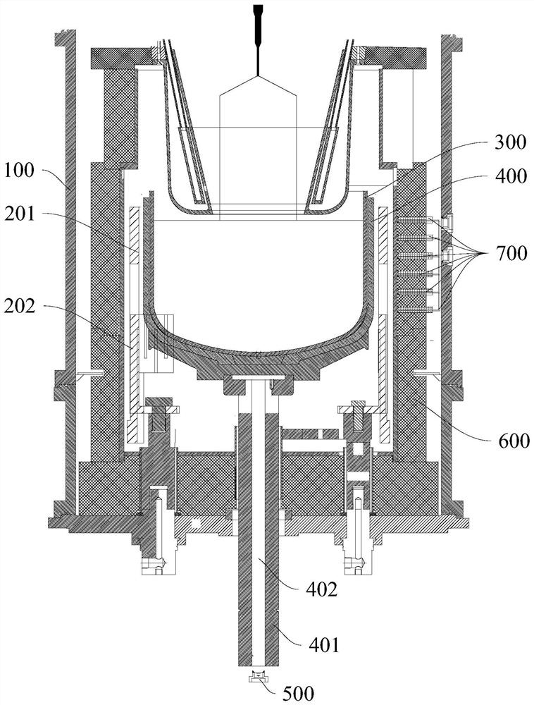
[0025] see figure 1 The crystal pulling furnace for semiconductor monocrystalline silicon in this embodiment includes a furnace body 100, a crucible and a heater 200 disposed in the furnace body 100, a gradient temperature measuring device is arranged in the furnace body, and a temperature tester is arranged at the bottom of the furnace body.

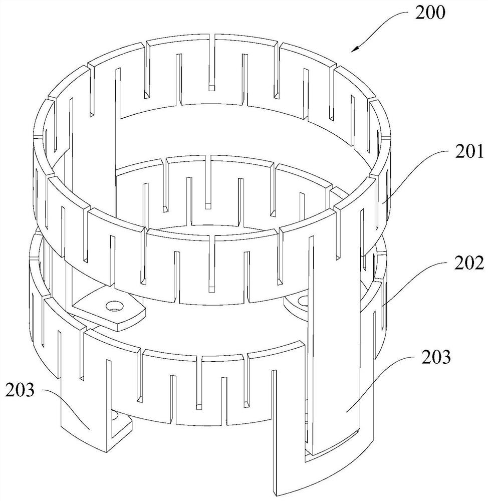
[0026] In this embodiment, the heater is arranged on the periphery of the crucible, including an upper heater 201 and a lower heater 202 arranged up and down at a certain distance. The height of the heating area of ​​the conventional thermal field heater covers the height of the entire melt in the quartz crucible. The height of the heating area of ​​the short thermal field heater is much smaller than the height of the melt in the crucible so as to achieve the effect of reducing oxygen. In this embodiment, two independently controlled upper heaters 201 and lower heaters 202 are arranged on the outside of the crucible. The upper and lower...


PUM


Abstract

The invention relates to a crystal pulling furnace for semiconductor monocrystalline silicon, and belongs to the technical field of monocrystalline silicon production. The crystal pulling furnace comprises a furnace body, a crucible and heaters, the crucible and the heater are arranged in the furnace body, a gradient temperature measuring device is arranged in the furnace body, and a temperature tester is arranged at the bottom of the furnace body; and the heaters are arranged on the periphery of the crucible and comprise an upper heater and a lower heater which are arranged up and down at a certain interval, the height of heating areas of the upper heater and the lower heater is 1 / 4-1 / 2 of the height of the crucible, and the interval between the heating areas of the upper heater and the lower heater is 50 mm to 1 / 3 of the height of the crucible. The temperature gradient of a melt in the crucible and the temperature of the bottom of the crucible are accurately controlled, so that high-quality silicon single crystals with low defect density and low COP are obtained, the requirements of various semiconductor silicon devices on the oxygen content of the single crystals are met, the stability and the consistency of the quality of the silicon single crystals are greatly improved, and an effective control method is provided for the crystal growth of the semiconductor silicon single crystals.

Description

technical field [0001] The invention relates to the technical field of monocrystalline silicon production, in particular to a crystal pulling furnace for semiconductor monocrystalline silicon. Background technique [0002] At present, the mainstream large-diameter semiconductor crystal pulling mainly adopts the superconducting magnetic field crystal pulling technology. The strong magnetic field of 3000-8000 Gauss greatly suppresses the convection of the silicon melt in the crucible, and the stability of the melt is greatly improved. Crystal growth can be realized at an extremely low crucible rotation of about 0.5rpm, the oxygen content in silicon can be reduced to below 12ppma, and the COP of various crystal defects and vacancy defect densities is also well controlled, but the low crucible rotation brings Obvious disadvantages such as the radial fluctuation caused by the asymmetry of the thermal field, the inhomogeneity of the melt temperature and impurity concentration caus...

Claims


Application Information

Patent Timeline
IPC IPC(8): C30B15/20C30B29/06
CPCC30B15/20C30B29/06
Inventor 姜益群
Owner 姜益群
Learn More