Heterojunction solar cell and preparation method thereof

A solar cell and heterojunction technology, applied in circuits, electrical components, photovoltaic power generation, etc., can solve the problem of affecting the short-circuit current and fill factor of heterojunction solar cells, increasing the production cost of heterojunction solar cells, and affecting the heterojunction Improve the efficiency of solar cells and other issues to achieve the effect of improving short-circuit current and fill factor, improving passivation effect, and avoiding high series resistance

Inactive Publication Date: 2021-07-02
ZHEJIANG AIKO SOLAR ENERGY TECH CO LTD +2
View PDF11 Cites 2 Cited by
  • Summary
  • Abstract
  • Description
  • Claims
  • Application Information

AI Technical Summary

Problems solved by technology

[0003] However, conventional heterojunction solar cells have problems such as high preparation costs and narrow process technology windows, which have led to the failure of large-scale commercial applications of heterojunction solar cells.
[0004] In addition, there are some structural defects in conventional heterojunction solar cells, which affect the efficiency of heterojunction solar cells. For example, in the heterojunction solar cell structure, transparent conductive thin film layer, intrinsic amorphous silicon layer and doped There is a large parasitic absorption and series resistance in the crystalline silicon layer, which greatly affects the short-circuit current and fill factor of the heterojunction solar cell; at the same time, due to the expensive equipment and high process cost of depositing the transparent conductive film layer, the Production cost of solar cells

Method used


Image

  • Heterojunction solar cell and preparation method thereof
  • Heterojunction solar cell and preparation method thereof
  • Heterojunction solar cell and preparation method thereof

Examples


preparation example Construction

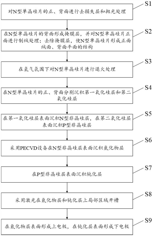
[0046] Correspondingly, see figure 2 As shown, the present invention also provides a method for preparing a heterojunction solar cell, comprising:

[0047] S1, removing the loss layer and polishing the front and back of the N-type single crystal silicon wafer;

[0048] Specifically, select an N-type single crystal silicon wafer with a thickness of 100-180 μm; clean the surface of the N-type single crystal silicon wafer to remove organic pollution and metal ions; Carry out sacrificial layer removal and polishing;

[0049] S2. Form a mask layer on the back side of the N-type single crystal silicon wafer, and perform texturing treatment on the front side of the N-type single crystal silicon wafer; remove the mask layer, so that the N-type single crystal silicon wafer forms a textured front surface and a flat back surface structure;

[0050] The structure of the back plane is formed by back polishing;

[0051] Specifically, a mask layer is formed on the back side of the N-typ...

Embodiment 1

[0075] S1, removing the loss layer and polishing the front and back of the N-type single crystal silicon wafer;

[0076] S2. Form a mask layer on the back side of the N-type single crystal silicon wafer, and perform texturing treatment on the front side of the N-type single crystal silicon wafer; remove the mask layer, so that the N-type single crystal silicon wafer forms a textured front surface and a flat back surface structure;

[0077] S3, performing annealing treatment on the N-type single crystal silicon wafer in a hydrogen atmosphere;

[0078] S4. Depositing a first silicon oxide layer and a second silicon oxide layer on the front and back sides of the N-type single crystal silicon wafer respectively, the thicknesses of the first silicon oxide layer and the second silicon oxide layer are both 2 nm;

[0079] S5. Depositing an N-type amorphous silicon layer on the surface of the first silicon oxide layer, depositing a P-type amorphous silicon layer on the surface of the ...

Embodiment 2

[0085] A method for preparing a heterojunction solar cell, comprising:

[0086] S1, removing the loss layer and polishing the front and back of the N-type single crystal silicon wafer;

[0087] S2. Form a mask layer on the back side of the N-type single crystal silicon wafer, and perform texturing treatment on the front side of the N-type single crystal silicon wafer; remove the mask layer, so that the N-type single crystal silicon wafer forms a textured front surface and a flat back surface structure;

[0088] S3, performing annealing treatment on the N-type single crystal silicon wafer in a hydrogen atmosphere;

[0089] S4. Depositing a first silicon oxide layer and a second silicon oxide layer respectively on the front and back of the N-type single crystal silicon wafer, the thickness of the first silicon oxide layer and the second silicon oxide layer are both 1 nm;

[0090] S5. Depositing an N-type amorphous silicon layer on the surface of the first silicon oxide layer, ...


PUM

PropertyMeasurementUnit
thicknessaaaaaaaaaa
thicknessaaaaaaaaaa
thicknessaaaaaaaaaa

Abstract

The invention discloses a heterojunction solar cell which comprises an N-type monocrystalline silicon wafer, and a first silicon oxide layer, an N-type amorphous silicon layer, a nitride layer and an upper electrode are sequentially arranged on the front face of the N-type monocrystalline silicon wafer. A second silicon dioxide layer, a P-type amorphous silicon layer, a passivation layer and a lower electrode are sequentially arranged on the back surface of the N-type monocrystalline silicon wafer; the N-type monocrystalline silicon wafer is of a structure with a suede front surface and a plane back surface; and the passivation layer is an aluminum oxide layer or a combination of the aluminum oxide layer and a silicon nitride layer. The invention also discloses a preparation method of the heterojunction solar cell, which is simple to operate and low in production cost. By adopting the heterojunction solar cell, parasitic absorption can be reduced, short-circuit current can be increased, and the heterojunction solar cell which is high in conversion efficiency, good in passivation effect and low in cost can be obtained.

Description

technical field [0001] The invention relates to the technical field of high-efficiency photovoltaic cells, in particular to a heterojunction solar cell and a preparation method thereof. Background technique [0002] Conventional heterojunction solar cells are made by depositing an amorphous silicon layer on an N-type crystalline silicon wafer. This structure can improve the performance of the PN junction, so that the conversion efficiency and open circuit voltage are improved. [0003] However, conventional heterojunction solar cells have problems such as high preparation cost and narrow process technology window, which have led to the failure of large-scale commercial application of heterojunction solar cells. [0004] In addition, there are some structural defects in conventional heterojunction solar cells, which affect the efficiency of heterojunction solar cells. For example, in the heterojunction solar cell structure, transparent conductive thin film layer, intrinsic am...

Claims


Application Information

Patent Timeline
Patent Type & Authority Applications(China)
IPC IPC(8): H01L31/0216H01L31/0236H01L31/0747H01L31/20
CPCH01L31/02167H01L31/02168H01L31/02363H01L31/0236H01L31/0747H01L31/202Y02P70/50Y02E10/50
Inventor 常纪鹏陈刚
Owner ZHEJIANG AIKO SOLAR ENERGY TECH CO LTD
Why Eureka
Try Eureka