
Eureka
For R&D, Eureka makes reading and utilizing patents & technical documents easy.
Eureka AIR
Designed for self-driven R&D workflows. Generate viable solutions, solve complex R&D challenges, empower your innovation with AI.

Eureka Materials
Designed for material experts only. Revolutionize your material R&D, from search, analyze, to developing new materials.

TechResearch
Generate reliable direction feasibility study reports for your R&D in just a few steps.

TechSeek
Discover and master advanced knowledge NOW. Basics, ideas, possibilities, all at once.

TechMind
As an expert in R&D Theories, TechMind can generates customized viable solutions instantly.

TechRisk
Analyze your overall solution with one click, know your potential R&D risks in advance.

TechMonitor
Get weekly tech updates, stay abreast of the latest tech innovations and key insights.
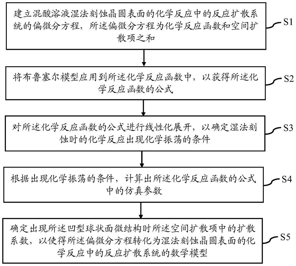
Wet etching process modeling method and manufacturing method of semiconductor device
A technology of wet etching and modeling method, applied in semiconductor/solid-state device manufacturing, instruments, electrical components, etc., can solve problems such as complex reaction mechanism, and achieve the effect of improving performance
- Summary
- Abstract
- Description
- Claims
- Application Information
AI Technical Summary
Problems solved by technology
Method used
Image

Examples
Embodiment Construction
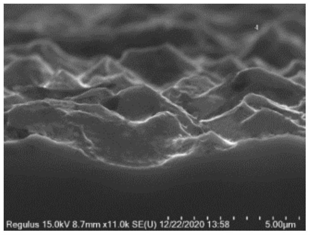
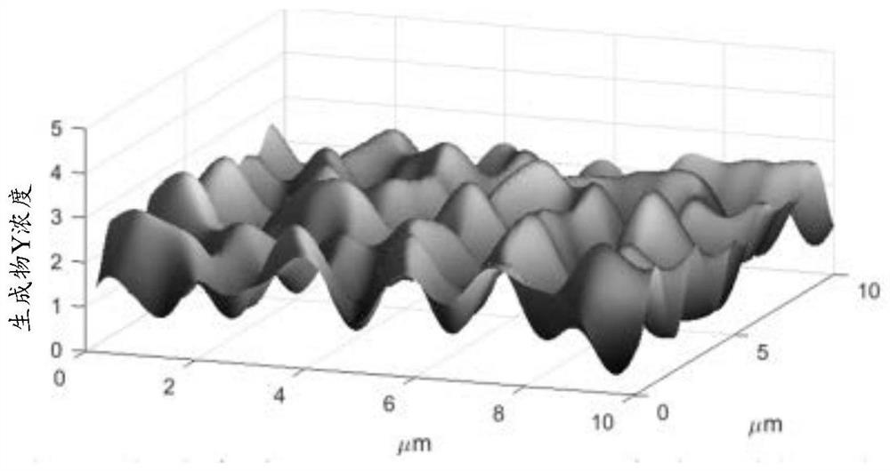
[0065] Take the wet etching of the silicon substrate on the back of the wafer with a mixed acid solution to form a concave spherical surface on the surface of the silicon substrate, thereby increasing the contact area with the metal electrode formed by sputtering metal to improve the overall adhesion of the interface , to explain the principle of wet etching to form a concave spherical surface:
[0066] Place the wafer in the acid tank of the cleaning machine or in the single wafer cleaning chamber to treat the silicon surface on the back of the wafer; during the reaction process, the temperature, the uniformity of mixed acid and the fluidity of the liquid are well controlled. In the system described above, reactants are transported from the main fluid to the boundary layer, diffuse to the silicon surface, and react, and products diffuse from the silicon surface to the boundary layer, and then transported to the main fluid.
[0067] At a set temperature, the microscopic moveme...
PUM
 Abstract
Description
Claims
Application Information
 - R&D Engineer
- R&D Manager
- IP Professional
- Industry Leading Data Capabilities
- Powerful AI technology
- Patent DNA Extraction
Browse by: Latest US Patents, China's latest patents, Technical Efficacy Thesaurus, Application Domain, Technology Topic, Popular Technical Reports.
© 2024 PatSnap. All rights reserved.Legal|Privacy policy|Modern Slavery Act Transparency Statement|Sitemap|About US| Contact US: help@patsnap.com