

Preparation method of indium tin oxide film pattern
A technology of indium tin oxide and thin film patterning, which is applied in the field of manufacturing, can solve the problems of ITO thin film resistance, irregular edges, over-etching, etc., and achieve the effect of solving uneven patterns, reducing preparation costs, and uniform patterns
- Summary
- Abstract
- Description
- Claims
- Application Information
AI Technical Summary
Problems solved by technology
Method used
Image

Examples
Embodiment 1
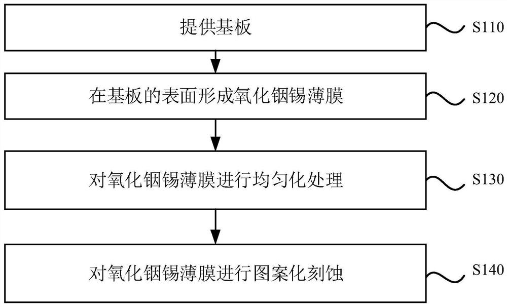
[0041] figure 1 The flow chart of the preparation of an indium tin oxide thin film pattern provided by Embodiment 1 of the present invention, this embodiment is applicable to the preparation of an indium tin oxide thin film pattern, see figure 1 , the preparation method of indium tin oxide film pattern comprises:
[0042] S110, providing a substrate.
[0043] Specifically, the substrate has the function of supporting and fixing, and the substrate can be a hard substrate, such as ordinary alkali glass, alkali-free glass, quartz glass or silicon substrate, etc., or a flexible substrate, such as polyimide (Polyimide, PI) Substrate, polyethylene naphthalate (PEN) substrate, polyethylene terephthalate (PET) substrate, polyethersulfone resin (PES) substrate, polycarbonate (PC) substrate or ultra-thin glass, etc. , the specific substrate can be selected according to the actual situation, for example, it can be selected according to the reliability of the substrate and the film laye...
Embodiment 2
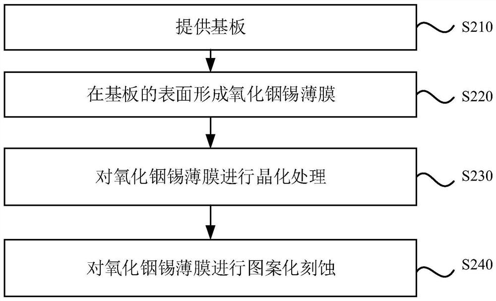
[0055] figure 2 A flow chart for the preparation of an indium tin oxide thin film pattern provided by Embodiment 2 of the present invention. This embodiment is applicable to the preparation of an indium tin oxide thin film pattern. Optionally, see figure 2 , the preparation method of indium tin oxide film pattern comprises:
[0056] S210, providing a substrate.
[0057] S220, forming an indium tin oxide thin film on the surface of the substrate.
[0058] S230, performing crystallization treatment on the indium tin oxide thin film.
[0059] Specifically, the indium tin oxide thin film is crystallized to make the indium tin oxide thin film crystallize. Compared with the amorphous indium tin oxide thin film, the mechanical strength of each part of the indium tin oxide thin film after crystallization is more uniform. Improve, so that the film has a uniform etching rate in each area in the subsequent patterned etching, and provide a guarantee for the regular edge etching morph...
Embodiment 3
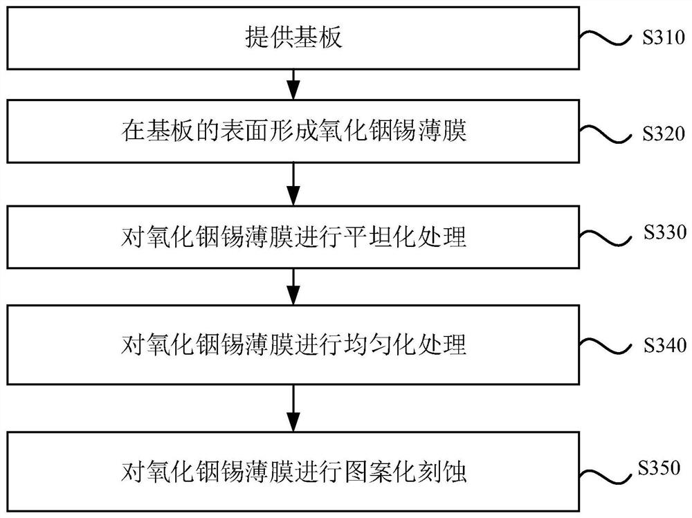
[0063] image 3 A flow chart for the preparation of an indium tin oxide thin film pattern provided by Embodiment 3 of the present invention. This embodiment is applicable to the preparation of an indium tin oxide thin film pattern. Optionally, see image 3 , the preparation method of indium tin oxide film pattern comprises:
[0064] S310, providing a substrate.
[0065] S320, forming an indium tin oxide thin film on the surface of the substrate.
[0066] S330, performing planarization treatment on the ITO thin film.
[0067] Specifically, after the indium tin oxide film is formed on the substrate, the indium tin oxide film is planarized to remove the burrs of the indium tin oxide film and reduce the roughness of the indium tin oxide film, so that the indium tin oxide film can be made The crystallization of the thin film is more uniform, fully crystallized, and the existence of amorphous structure is avoided.
[0068] Optionally, S330, performing planarization treatment on ...
PUM
| Property | Measurement | Unit |
|---|---|---|
| Thickness | aaaaa | aaaaa |
| Thickness | aaaaa | aaaaa |
| Thickness | aaaaa | aaaaa |
Abstract
Description
Claims
Application Information