Supercharge Your Innovation With Domain-Expert AI Agents!

Flexible two-dimensional material optical detector array and manufacturing method thereof

A two-dimensional material, photodetector technology, applied in metal material coating process, semiconductor device, final product manufacturing and other directions, can solve the problems of poor environmental stability, adsorption of impurities, easy oxidation and decomposition, etc., to achieve low dark current. Effect

Active Publication Date: 2021-07-20
BEIJING INSTITUTE OF TECHNOLOGYGY
View PDF3 Cites 0 Cited by
  • Summary
  • Abstract
  • Description
  • Claims
  • Application Information

AI Technical Summary

Problems solved by technology

[0004] However, the preparation and device performance of two-dimenSional layered materials (2DLMS) still face many common challenges: how to obtain high-quality and uniform materials; how to control the orientation, thickness and morphology of crystals; How to optimize device structure; how to achieve on-chip integration; how to maximize photosensitivity; how to improve repeatability
Although two-dimensional materials have excellent properties that are expected, their environmental stability is poor, and their performance cannot be maintained after deviceization. They are prone to oxidative decomposition and adsorption of impurities in the atmospheric environment.

Method used


Image

  • Flexible two-dimensional material optical detector array and manufacturing method thereof
  • Flexible two-dimensional material optical detector array and manufacturing method thereof
  • Flexible two-dimensional material optical detector array and manufacturing method thereof

Examples


Embodiment Construction

[0048] The present invention will be described in detail below with reference to the accompanying drawings and examples.

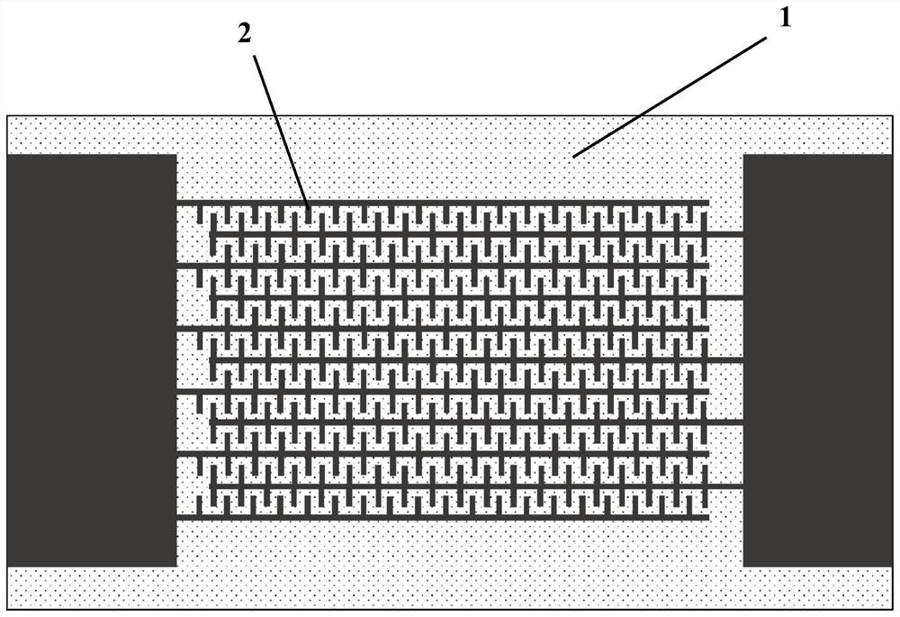
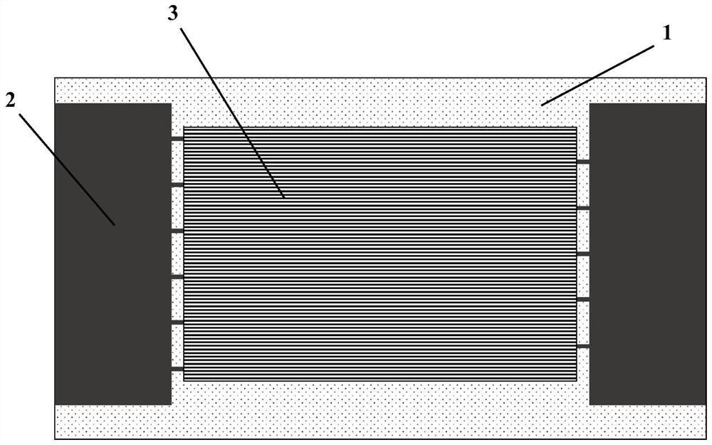
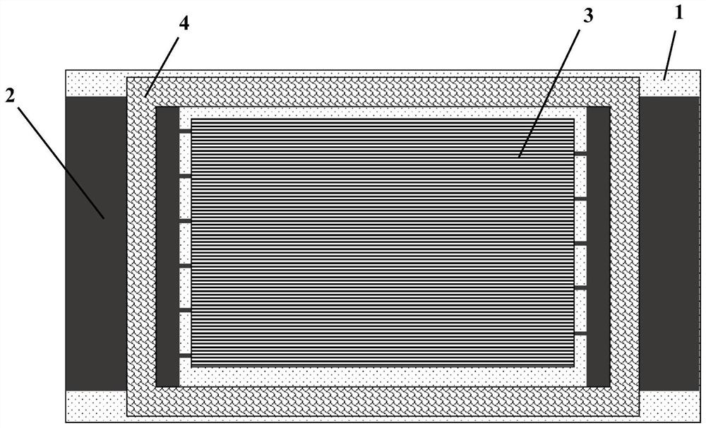
[0049] A flexible two-dimensional material photodetector array of the present invention has a structure from bottom to top: a flexible transparent substrate, an interdigitated transparent electrode array, a two-dimensional material photosensitive layer, and a flexible transparent insulating packaging cover plate. Wherein, the area of ​​the flexible transparent substrate at the bottom layer is larger than that of the flexible transparent insulating package cover plate at the top layer, so as to facilitate packaging and lead out electrodes, and the substrate and the cover plate are connected and sealed by epoxy resin-polyimide adhesive.

[0050] A method for manufacturing a flexible two-dimensional material photodetector array of the present invention comprises the following steps:

[0051] Step S1, preparing the bottom flexible transparent substrate and the...


PUM


Abstract

The invention provides a flexible two-dimensional material optical detector array and a manufacturing method thereof. The flexible two-dimensional material optical detector array can stably work at room temperature and in an atmospheric environment. According to the flexible two-dimensional material optical detector array, the two-dimensional material NbSe2 generally has a triangular prism structure (2H phase) or an octahedral structure (1T phase), the 2H phase is semimetal, the 1T phase is a Mott insulator, a grown large-area or bulk material is generally the 2H phase, and a semimetal film of the 2H phase is suitable for being used as a photosensitive layer material of a photoelectric device due to the photoconductive characteristic of the semimetal film. And compared with a bulk material, the material has lower dark current and has response to illumination in a spectral range of 532nm to 808nm.

Description

technical field [0001] The invention belongs to the technical field of two-dimensional material photodetectors, and in particular relates to a flexible two-dimensional material photodetector array and a manufacturing method thereof. Background technique [0002] Photodetectors are devices that convert light signals (electromagnetic radiation carrying energy) into precise electrical signals (usually photocurrent and photovoltage), and high-performance photodetection technology is very important in both science and industry It has a wide range of applications in video imaging, optical communication, fire monitoring, biomedical imaging, environmental monitoring, space detection, security, night vision and motion detection. At present, most photodetectors on the market are assembled based on bulk crystalline silicon, which can work in the visible and near-infrared ranges; there are also photodetectors based on three-dimensional materials such as: silicon / Germanium (Si / Ge) hete...

Claims


Application Information

Patent Timeline
Patent Type & Authority Applications(China)
IPC IPC(8): H01L31/0224H01L31/18H01L31/0203C23C14/02C23C14/06C23C14/08C23C14/28C23C14/35
CPCH01L31/022408H01L31/0203H01L31/022475H01L31/1884C23C14/28C23C14/35C23C14/086C23C14/0623C23C14/022Y02P70/50
Inventor 许自强刘立巍王业亮候延辉黄泽平杨涵张全震张腾
Owner BEIJING INSTITUTE OF TECHNOLOGYGY
Features
  • R&D
  • Intellectual Property
  • Life Sciences
  • Materials
  • Tech Scout
  • Unparalleled Data Quality
  • Higher Quality Content
  • 60% Fewer Hallucinations
Learn More