Preparation method of vertical nanowire array

A nanowire array and sacrificial layer technology, applied in the field of preparation of vertical nanowire arrays, can solve problems such as affecting the electrical properties of nanowires, high cost, incompatibility, etc., and achieve controllable size and distance, high preparation efficiency, and array geometry. The effect of precise shape control

Pending Publication Date: 2021-07-27
INST OF MICROELECTRONICS CHINESE ACAD OF SCI
View PDF9 Cites 1 Cited by
  • Summary
  • Abstract
  • Description
  • Claims
  • Application Information

AI Technical Summary

Problems solved by technology

Electron beam exposure and etching schemes have low preparation efficiency and high cost, and cannot be used for large-scale preparation and application; VLS synthesis can prepare single-crystal silicon nano-nanowires. During the synthesis process, the metal catalyst gold will diffuse into the nanowires, affecting the nanostructures. The electrical properties of the wires are not compatible with cmos; the preparation of dispersed silicon nanowires by the solution-liquid-solid (SLS) method has the advantages of low cost and large-scale production potential, but it is difficult to prepare highly ordered VA-SiNW arrays; metal Silicon nanostructures with high structural fidelity and purity can be fabricated by metal-assisted chemical etching (MACE), however, it is difficult to control the size and uniformity of nanoarrays by metal-assisted chemical etching

Method used


Image

  • Preparation method of vertical nanowire array
  • Preparation method of vertical nanowire array
  • Preparation method of vertical nanowire array

Examples


Embodiment Construction

[0038] Hereinafter, embodiments of the present invention will be described with reference to the drawings. It should be understood, however, that these descriptions are exemplary only and are not intended to limit the scope of the present invention. Also, in the following description, descriptions of well-known structures and techniques are omitted to avoid unnecessarily obscuring the concept of the present invention.

[0039] Various structural schematic diagrams according to embodiments of the present invention are shown in the drawings. The figures are not drawn to scale, with certain details exaggerated and possibly omitted for clarity of presentation. The shapes of the various regions and layers shown in the figure, as well as their relative sizes and positional relationships are only exemplary, and may deviate due to manufacturing tolerances or technical limitations in practice, and those skilled in the art will Regions / layers with different shapes, sizes, and relative...


PUM

PropertyMeasurementUnit
lengthaaaaaaaaaa

Abstract

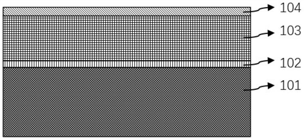
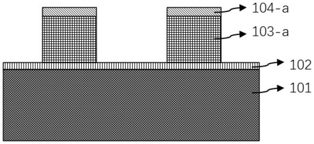
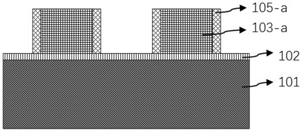
The invention relates to a preparation method of a vertical nanowire array, which comprises the following steps of: forming a nanoscale two-layer side wall cross array by adopting a two-time self-aligned side wall transfer technology, forming a silicon nitride nano dot array by utilizing the selection ratio of silicon oxide to silicon nitride and reactive ion etching (RIE) of the height difference of the cross position of the secondary side wall array, preparing a silicon nitride dot matrix array, etching substrate silicon by taking the silicon nitride dot matrix array as a mask to form a vertical nanowire array, and finally corroding residual silicon nitride and silicon oxide by using an acid solution to prepare the high-purity, damage-free, orderly and vertically arranged silicon nanowires.

Description

technical field [0001] The invention relates to the technical field of semiconductor integration, in particular to a preparation method of a vertical nanowire array. Background technique [0002] Vertical nanowires (V-SiNWs) are key structures for the fabrication and development of transistors, MEMS, optical sensors, and silicon-based batteries. Vertical silicon nanowire arrays, a special silicon nanostructure, have shown great potential in next-generation photovoltaic, photocatalytic, and sensor devices. [0003] However, at present, the preparation methods of V-SiNW arrays include electron beam lithography and etching, vapor-liquid-solid (VLS) synthesis, solution-liquid-solid (SLS) synthesis, reactive ion etching and metal-assisted chemical etching. Preparation of silicon nanowires. Electron beam exposure and etching schemes have low preparation efficiency and high cost, and cannot be used for large-scale preparation and application; VLS synthesis can prepare single-crys...

Claims


Application Information

Patent Timeline
Patent Type & Authority Applications(China)
IPC IPC(8): B81C1/00B81B7/00B81B7/04
CPCB81C1/00031B81B7/0009B81B7/04
Inventor 田佳佳张青竹李俊杰吴次南张兆浩殷华湘张静王文武
Owner INST OF MICROELECTRONICS CHINESE ACAD OF SCI
Why Eureka
Try Eureka