Tunneling magnetoresistive biosensor and preparation method and application thereof
A biosensor and tunneling magneto-resistance technology, applied in magnetic sensor arrays, instruments, scientific instruments, etc., can solve the problems of low sensitivity of colloidal gold method and easy occurrence of missed detection, so as to improve detection sensitivity and detection rate , Improve the effect of signal-to-noise ratio
- Summary
- Abstract
- Description
- Claims
- Application Information
AI Technical Summary
Problems solved by technology
Method used
Image
Examples
Embodiment 1
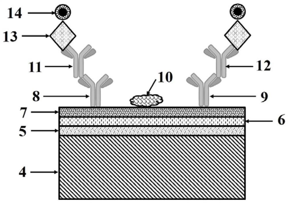
[0049] (1) The tunneling magnetoresistive sensor chip is composed of a CoFe / CoFeB / MgO / CoFeB multilayer film on a silicon wafer, which is in a zigzag shape. The multilayer film structure is deposited by magnetron sputtering, and the CoFe and MgO layers are passed through radio frequency pattern deposition.
[0050] (2) Plating a protective layer of Al on the surface of the tunneling magnetoresistive sensor by atomic layer deposition 2 o 3 , Al 2 o 3 The thickness is 20nm.
[0051] (3) In the protective layer Al 2 o 3 A protective layer and a biological binding layer SiO are plated on the surface by plasma chemical vapor deposition 2 , SiO 2 The thickness is 20nm.
[0052] (4) Wash the tunneling magnetoresistive sensor three times with acetone, methanol, and isopropanol for 10 minutes, dry with nitrogen, and treat with oxygen plasma for 30 minutes. The treated sensor was treated in 2% (3-aminopropyl) triethoxysilane (absolute ethanol) solution for 30 minutes, dried in a...
Embodiment 2
[0056] (1) The tunneling magnetoresistive sensor chip is composed of a CoFe / CoFeB / MgO / CoFeB multilayer film on a silicon wafer, which is in a zigzag shape. The multilayer film structure is deposited by magnetron sputtering, and the CoFe and MgO layers are passed through radio frequency pattern deposition.
[0057] (2) Plating a protective layer of Al on the surface of the tunneling magnetoresistive sensor by atomic layer deposition 2 o 3 , Al 2 o 3 The thickness is 18nm.
[0058] (3) In the protective layer Al 2 o 3 A protective layer and a biological binding layer SiO are plated on the surface by plasma chemical vapor deposition 2 , SiO 2 The thickness is 20nm.
[0059] (4) Wash the tunneling magnetoresistive sensor three times with acetone, methanol, and isopropanol for 10 minutes, dry with nitrogen, and treat with oxygen plasma for 30 minutes. The processed sensor was treated in 5% (3-aminopropyl) triethoxysilane (absolute ethanol) solution for 1 hour, dried in an ...
Embodiment 3
[0063] (1) The tunneling magnetoresistive sensor chip is composed of a CoFe / CoFeB / MgO / CoFeB multilayer film on a silicon wafer, which is in a zigzag shape. The multilayer film structure is deposited by magnetron sputtering, and the CoFe and MgO layers are passed through radio frequency pattern deposition.
[0064] (2) Plating a protective layer of Al on the surface of the tunneling magnetoresistive sensor by atomic layer deposition 2 o 3 , Al 2 o 3 The thickness is 20nm.
[0065] (3) In the protective layer Al 2 o 3 A protective layer and a biological binding layer SiO are plated on the surface by plasma chemical vapor deposition 2 , SiO 2 The thickness is 50nm.
[0066] (4) Wash the tunneling magnetoresistive sensor three times with acetone, methanol, and isopropanol for 10 minutes, dry with nitrogen, and treat with oxygen plasma for 30 minutes. The treated sensor was treated in 2% (3-aminopropyl) triethoxysilane (absolute ethanol) solution for 1 hour, dried in an ov...
PUM
| Property | Measurement | Unit |
|---|---|---|
| Thickness | aaaaa | aaaaa |
| Diameter | aaaaa | aaaaa |
| Thickness | aaaaa | aaaaa |
Abstract
Description
Claims
Application Information

