Epitaxial growth method for improving crystal quality of aluminum nitride material, and aluminum nitride material

An epitaxial growth and crystal quality technology, applied in crystal growth, polycrystalline material growth, single crystal growth and other directions, can solve the problems of good balance, low yield, poor uniformity, etc. Quality-improving, widely adaptable effects

Pending Publication Date: 2021-08-20
SUZHOU INST OF NANO TECH & NANO BIONICS CHINESE ACEDEMY OF SCI
View PDF10 Cites 3 Cited by
  • Summary
  • Abstract
  • Description
  • Claims
  • Application Information

AI Technical Summary

Problems solved by technology

Although such methods can effectively improve the quality of AlN thin film epitaxial crystals, the process is complicated and the process is numerous.
As a result, AlN thin film products not only increase the cost significantly, but also have low yield and poor uniformity, so this method is difficult to be practically applied to large-scale industrial production
Therefore, although other methods such as lateral epitaxy and pulsed atomic layer epitaxy can improve the quality of AlN thin film crystals to a certain extent, they are often time-consuming and complicated, resulting in high costs in actual production.
[0006] In summary, it can be found that the above-mentioned existing high-quality AlN epitaxial film growth methods mainly focus on improving the surface mobility of Al atoms, and hope to reduce the dislocation density by effecting GaN two-step growth, but the effect is either not ideal or obvious, The quality of the grown AlN is still poor, or the process is complex, requiring patterned substrates, secondary epitaxy and other processes, resulting in a series of problems such as cost and uniformity, and it is impossible to achieve a good balance between practicability and effect

Method used


Image

  • Epitaxial growth method for improving crystal quality of aluminum nitride material, and aluminum nitride material
  • Epitaxial growth method for improving crystal quality of aluminum nitride material, and aluminum nitride material
  • Epitaxial growth method for improving crystal quality of aluminum nitride material, and aluminum nitride material

Examples


Embodiment 1

[0079] Example 1 Preparation of high-quality AlN epitaxial film on silicon substrate

[0080] S1. Substrate heat treatment: Put Si(111) substrate into MOCVD, 2 Under the atmosphere, raise the temperature to 1150°C, and then heat-treat for 5 minutes to remove the surface oxide layer.

[0081] S2. Pre-spread Al: reduce the growth temperature to 1050°C and maintain pure H 2 Under the conditions, the Al source is introduced, and a layer of Al is spread on the surface of the substrate to prevent NH 3 in contact with the substrate.

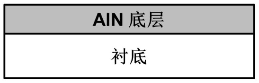
[0082] S3, growing the bottom layer of AlN: after laying Al, pass NH 3 , under the growth conditions of 1050°C, V / III of 200, and pressure of 50mbar, a 300nm AlN bottom layer was grown.

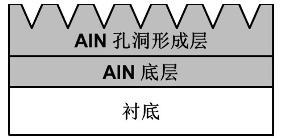
[0083] S4. Growth of AlN hole-forming layer: reduce the growth temperature to 850°C, increase V / III ratio to 2000, and pressure 100mbar, and grow 200nm AlN hole-forming layer at low temperature and high V / III to form diamond-shaped holes with crystal planes on the ...

Embodiment 2

[0086] Example 2 Preparation of high-quality AlN epitaxial film on planar sapphire substrate

[0087] S1. Sputtering an AlN bottom layer: On a sapphire substrate, sputter a 50nm AlN thin film as an AlN bottom layer.

[0088] S2. Put the AlN bottom layer into MOCVD, raise the temperature to 1150°C, and feed H at the same time 2 and NH 3 , annealed at high temperature for 10 minutes.

[0089] S3. Growth of AlN hole-forming layer: reduce the growth temperature to 900°C, increase the V / III ratio to 5000, and pressure 300mbar, and grow a 300nm AlN hole-forming layer at low temperature and high V / III to form diamond-shaped holes with crystal planes on the inner wall for The hole diameter is about 100nm.

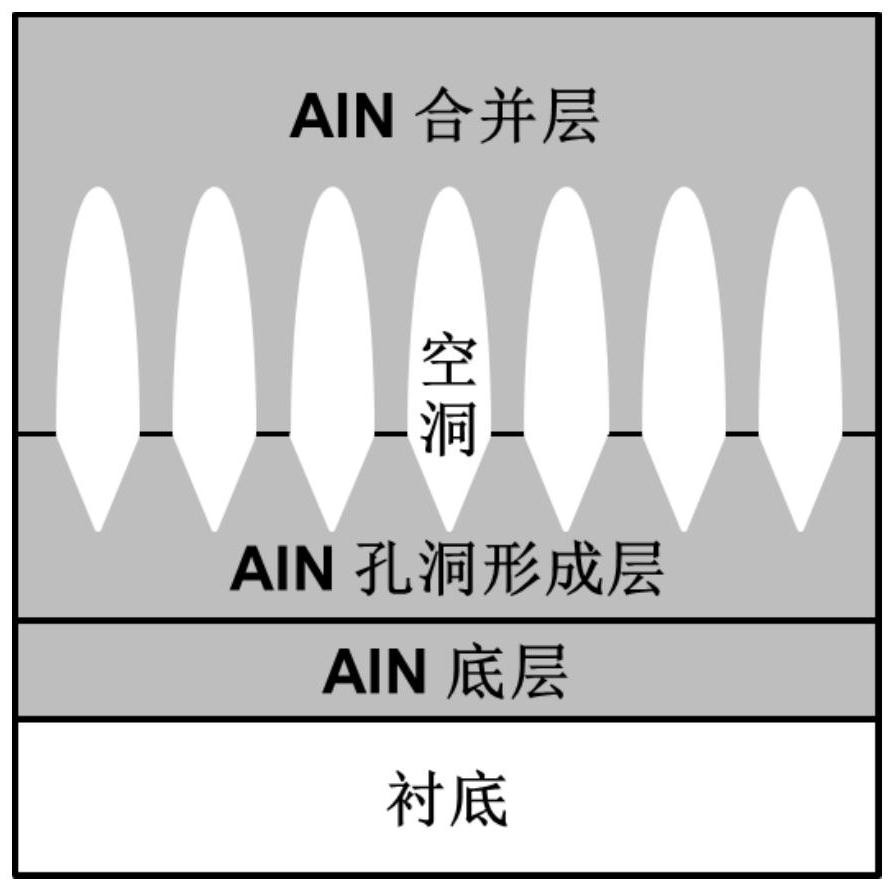
[0090] S4. Growth of AlN merged layer: increase the growth temperature to 1200°C, reduce V / III ratio to 50, pressure 30mbar, grow 700nm AlN merged layer at high temperature and low V / III, and form voids inside the material, with an average width of 90nm , the vertical depth i...

Embodiment 3

[0093] Example 3 Preparation of high quality and high Al composition AlGaN epitaxial thin film on silicon substrate

[0094] S1. Substrate heat treatment: Put Si(111) substrate into MOCVD, 2 Under the atmosphere, raise the temperature to 1150°C, and then heat-treat for 5 minutes to remove the surface oxide layer.

[0095] S2. Pre-spread Al: reduce the growth temperature to 1050°C and maintain pure H 2 Under the conditions, the Al source is introduced, and a layer of Al is spread on the surface of the substrate to prevent NH 3 in contact with the substrate.

[0096] S3, growing the bottom layer of AlN: after laying Al, pass NH 3 , under the growth conditions of 1050°C, V / III of 200, and pressure of 50mbar, a 200nm AlN bottom layer was grown.

[0097] S4. Growing the bottom layer of AlGaN: on the basis of the bottom layer of AlN, pass NH at the same time 3 , Al source, Ga source, under the conditions of growth temperature of 1100°C, growth pressure of 100mbar, and growth V / ...


PUM

PropertyMeasurementUnit
Total thicknessaaaaaaaaaa
Thicknessaaaaaaaaaa

Abstract

The invention discloses an epitaxial growth method for improving the crystal quality of an aluminum nitride material, and the aluminum nitride material. The epitaxial growth method for improving the crystal quality of the aluminum nitride material comprises the following steps: growing and forming an aluminum nitride bottom layer on a substrate, growing an aluminum nitride hole forming layer on the aluminum nitride bottom layer, and simultaneously forming a plurality of holes in the aluminum nitride hole forming layer; and growing an aluminum nitride merging layer on the aluminum nitride hole forming layer, merging materials for forming the aluminum nitride merging layer at the top of each hole to form a cavity in situ, and wrapping the cavity in the aluminum nitride merging layer to make the epitaxial layer formed on the cavity have a flat and crack-free surface. The epitaxial growth method for improving the quality of the AlN material has the advantages of remarkable dislocation density reduction effect, capability of simultaneously inhibiting cracks, simple process, wide adaptability and the like, so that the thicker crack-free and high-quality AlN material grows, and the epitaxial growth method is completely suitable for commercial production.

Description

technical field [0001] The invention relates to the technical field of semiconductor material growth, in particular to an epitaxial growth method for improving the crystal quality of aluminum nitride (AlN) material and the obtained high-quality aluminum nitride material. Background technique [0002] AlN single crystal materials have a large band gap (6.2eV) and a direct bandgap energy band structure, so they are very suitable for deep ultraviolet optoelectronic devices, such as light-emitting diodes, lasers, detectors, etc. At the same time, AlN single crystal material also has excellent characteristics such as high breakdown voltage and small dielectric constant, which makes it have important application value in the field of power electronic devices. In addition, high-quality AlN single crystal materials are also the key to fabricate high-performance filters. [0003] Due to the difficulty in preparing AlN bulk single crystals and the small available size and high market...

Claims


Application Information

Patent Timeline
IPC IPC(8): C30B25/04C30B25/18C30B29/38C23C16/34C23C16/44C23C16/04
CPCC30B25/04C30B25/18C30B29/38C23C16/34C23C16/44C23C16/04
Inventor 孙钱黄应南刘建勋孙秀建詹晓宁高宏伟杨辉
Owner SUZHOU INST OF NANO TECH & NANO BIONICS CHINESE ACEDEMY OF SCI
Why Eureka
Try Eureka