
Asymmetric MOSFET, manufacturing method thereof and semiconductor device

A manufacturing method and semiconductor technology, applied in semiconductor devices, semiconductor/solid-state device manufacturing, transistors, etc., can solve the problem that asymmetric MOSFETs cannot meet higher speed and smaller size at the same time, so as to increase the difficulty of control and increase the richness , The effect of fast switching speed

Inactive Publication Date: 2021-08-24
MICROTERA SEMICON (GUANGZHOU) CO LTD
View PDF7 Cites 4 Cited by
  • Summary
  • Abstract
  • Description
  • Claims
  • Application Information

AI Technical Summary

Problems solved by technology

[0004] However, in the face of higher requirements for size reduction, such as shrinking below 30 nm, bulk silicon-based asymmetric MOSFETs cannot meet the requirements of higher speed and smaller size at the same time

Method used


Image

  • Asymmetric MOSFET, manufacturing method thereof and semiconductor device
  • Asymmetric MOSFET, manufacturing method thereof and semiconductor device
  • Asymmetric MOSFET, manufacturing method thereof and semiconductor device

Examples


Embodiment 1

[0111] This embodiment provides a method for manufacturing an asymmetric MOSFET, such as Figure 5 As shown, the method includes the following steps:

[0112] Step S101: providing a substrate, the substrate includes a semiconductor base, a buried oxide layer formed on the semiconductor base, and a semiconductor layer formed above the buried oxide layer, a gate structure is formed above the semiconductor layer, forming lightly doped regions of a source region and a drain region in the semiconductor layer around the gate;

[0113] Such as Figure 6 As shown, the substrate provided in this embodiment includes a semiconductor substrate 100 , a buried oxide layer 101 located above the semiconductor substrate 100 , and a semiconductor layer 102 located above the buried oxide layer 101 . In this embodiment, the substrate is silicon-on-insulator (SOI), that is, the semiconductor substrate 100 is a silicon substrate, the semiconductor layer 102 is silicon, and the buried oxide layer ...

Embodiment 2

[0132] In this embodiment, a method for manufacturing an asymmetric MOSFET is also provided. The difference from Embodiment 1 is that in this embodiment, a Figure 9 After the photoresist layer 140 is shown, as Figure 12 As shown, under the cover of the photoresist layer 140 , when the source isolation spacer is etched, the source isolation spacer is completely removed, and only the drain isolation spacer 113 remains. Then the photoresist layer 140 is removed, and the second doped region of the source region and the first doped region of the drain region are heavily doped. Such as Figure 13 As shown, heavily doped regions 122 and 112 are formed in the source region and the drain region, respectively. Since the source isolation spacer has been completely removed, and only the drain isolation spacer remains, the second doped region of the source region is completely converted into a heavily doped region 122, and the drain region is blocked by the drain isolation spacer 113. ...

Embodiment 3

[0135] This embodiment also provides a method for manufacturing an asymmetric MOSFET, and the similarities with Embodiment 1 and Embodiment 2 will not be repeated, and the difference lies in:

[0136] in formation Figure 8 After the structure shown, as in Figure 17 As shown, the source isolation spacer is dry-etched, and the dry-etched ion beam 170 is incident on the source isolation spacer 123 at a predetermined inclination angle α. In this embodiment, the source isolation spacer 123 is defined as the angle between the ion beam and the Y direction perpendicular to the substrate surface. The inclination angle α is between 35°-90°, more preferably, between 60°-80°. In this method, the etching removal amount of the source isolation sidewall is controlled by controlling the etching time, the angle of the inclination angle and the like. For example, in the 180nm CMOS process, the source isolation spacer and the drain isolation spacer are Si 3 N 4 , control the inclination a...


PUM

PropertyMeasurementUnit
thicknessaaaaaaaaaa
thicknessaaaaaaaaaa
thicknessaaaaaaaaaa

Abstract

The invention provides an asymmetric MOSFET, a manufacturing method thereof and a semiconductor device. The asymmetric MOSFET is formed on a silicon-on-insulator substrate, and the length of a lightly doped region of a source region is smaller than that of a lightly doped region of a drain region, or the source region is not provided with the lightly doped region. Due to the characteristics of the silicon-on-insulator substrate, the silicon-on-insulator can realize a shallower source-drain junction than bulk silicon, so that a transistor with a higher speed can be manufactured. Especially for a transistor process of less than 30nm, the silicon-on-insulator is an excellent solution for improving the speed of the transistor. The manufacturing method provided by the invention is compatible with the traditional asymmetric MOSFET manufacturing process, and the cost is not increased in the whole process. The different arrangement modes of the asymmetric MOSFETs in the semiconductor device do not need to add a photomask, the complexity of process control and the control difficulty of an inclination angle are not increased, and meanwhile, the richness in actual circuit use is increased.

Description

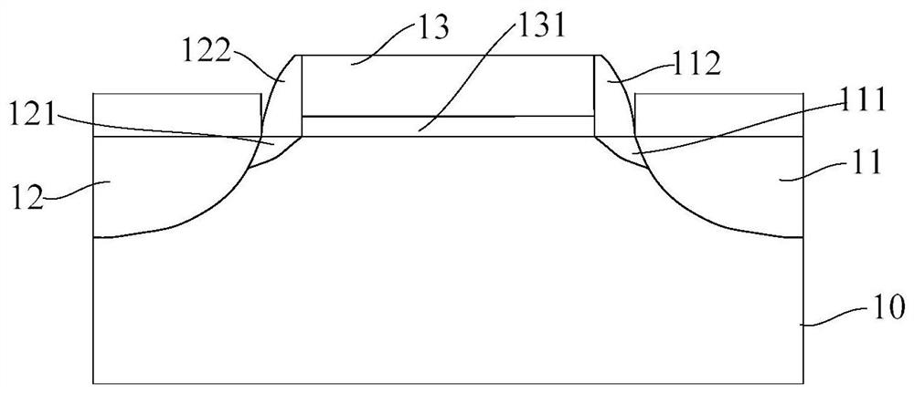
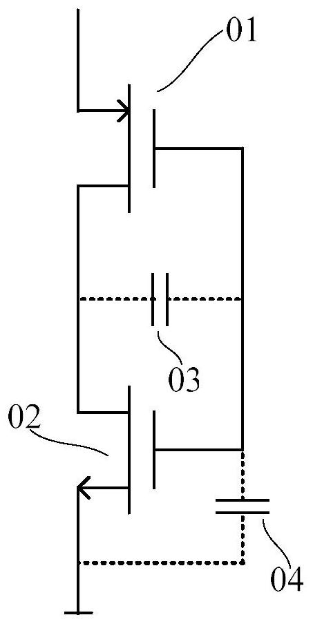
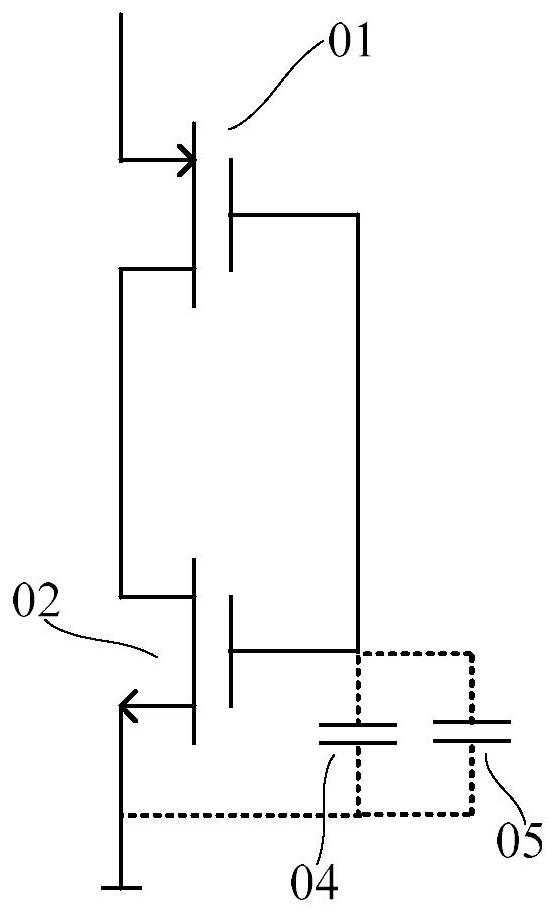
technical field [0001] The invention relates to the field of manufacturing integrated circuit semiconductor devices, in particular to an asymmetric MOSFET, a manufacturing method thereof and a semiconductor device. Background technique [0002] With the advent of fifth-generation communications, the Internet of Things, and big data, integrated circuits are increasingly demanding speed. The reduction of the channel length of transistors represented by Moore's Law has brought performance improvements, but when the size of transistors is further reduced, the room for speed improvement brought about by the reduction of channel lengths is getting smaller and smaller. [0003] In the cross-sectional view of a traditional symmetrical Metal-Oxide-Semiconductor Field Effect Transistor (MOSFET), due to the Miller effect, the capacitance at the drain end is equivalent to the capacitance at the output end will double. The multiplication of the drain terminal capacitance caused by the M...

Claims


Application Information

Patent Timeline
Patent Type & Authority Applications(China)
IPC IPC(8): H01L21/336H01L29/786H01L27/088
CPCH01L29/78624H01L29/78603H01L29/66742H01L27/088H01L29/6653H01L29/7835H01L29/66659
Inventor 刘森戴彬史林森刘筱伟
Owner MICROTERA SEMICON (GUANGZHOU) CO LTD
Learn More