Polycrystalline silicon thin film containing silicon-oxygen nanocrystalline layer and preparation method and application of polycrystalline silicon thin film
A polycrystalline silicon thin film and nanocrystalline layer technology, applied in the field of solar cells, can solve the problems of passivation quality degradation, large recombination current, etc., and achieve the effects of slowing diffusion, reducing recombination current, and improving passivation performance
- Summary
- Abstract
- Description
- Claims
- Application Information
AI Technical Summary
Problems solved by technology
Method used
Image
Examples
Embodiment 1
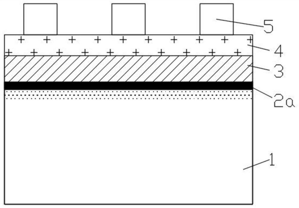
[0051] Such as figure 1 As shown, this embodiment provides a polysilicon thin film containing a silicon-oxygen nanocrystalline layer, including a tunneling layer on the back of the substrate 1, a doped polysilicon layer 3 on the back of the tunneling layer, and a doped polysilicon layer 3 on the back of the tunneling layer. The sintered electrode 5 on the back side also includes a first silicon-oxygen nanocrystal layer 4 between the doped polysilicon layer 3 and the sintered electrode 5, the first silicon-oxygen nanocrystal layer 4 is used to suppress the metal of the sintered electrode 5 diffusion.
[0052] Further, the doped oxygen content of the first silicon-oxygen nanocrystal layer 4 ranges from 5at% to 50at%; and / or, the first silicon-oxygen nanocrystal layer 4 has an electrically active impurity doping concentration in the range of 1E18-1E21cm -3 and / or, the thickness of the first silicon-oxygen nanocrystal layer 4 is 2-100 nm; and / or, the crystallization rate of the s...
Embodiment 2
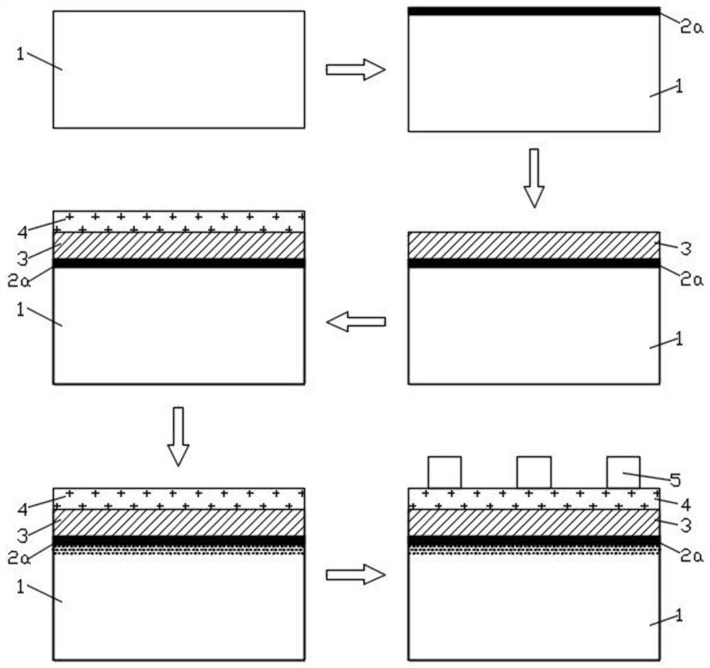
[0068] Such as figure 2 As shown, this embodiment provides a preparation method for preparing the structure of the polysilicon thin film containing the silicon oxygen nanocrystalline layer in Example 1. On the back of the substrate 1, the tunneling layer, the doped polysilicon precursor, and the first silicon Oxygen nanocrystal precursor, metal paste;
[0069] Finally, high-temperature annealing is performed, and the doped polysilicon precursor and the first silicon-oxygen nanocrystal precursor are correspondingly formed into a doped polysilicon layer 3 and a first silicon-oxygen nanocrystal layer 4 to obtain a sample a.
[0070] Further, the specific preparation method of this embodiment is as follows: p-type silicon wafer substrate 1, cleaning, double-sided alkali polishing, using PECVD in-situ oxidation method to prepare ultra-thin silicon oxide layer 2a on the front and back sides of the silicon wafer, using PECVD method on the A 40nm boron-doped amorphous silicon film i...
Embodiment 3
[0075] Such as Figure 4 As shown, this embodiment is different from Embodiment 1 in that this embodiment also includes a first polysilicon layer 6, and the first polysilicon layer 6 is located between the first silicon-oxygen nanocrystal layer 4 and the between the sintered electrodes 5 .
[0076] Further, the first polysilicon layer 6 is deposited on the surface of the first silicon-oxygen nanocrystalline layer 4 , and the sintered electrode 5 is screen-printed on the surface of the first polysilicon layer 6 .
[0077] Furthermore, the first polycrystalline silicon layer 6 , the first silicon-oxygen nanocrystalline layer 4 and the doped polycrystalline silicon layer 3 are deposited together, and then annealed together to form their respective structures.
PUM
| Property | Measurement | Unit |
|---|---|---|
| thickness | aaaaa | aaaaa |
| thickness | aaaaa | aaaaa |
| thickness | aaaaa | aaaaa |
Abstract
Description
Claims
Application Information


