Oxide semiconductor device and production method thereof

An oxide semiconductor and device technology, applied in semiconductor devices, semiconductor/solid-state device manufacturing, transistors, etc., can solve problems such as short channel effect, small carrier mobility and on-state current, and limited device performance improvement. , to achieve the effect of simple process, improvement of sub-threshold characteristics, and suppression of short channel effect

Pending Publication Date: 2021-10-01
INST OF MICROELECTRONICS CHINESE ACAD OF SCI
View PDF0 Cites 0 Cited by
  • Summary
  • Abstract
  • Description
  • Claims
  • Application Information

AI Technical Summary

Problems solved by technology

However, due to the large number of deep-level defect states in the OS film and the limitation of its conductive mechanism, the carrier mobility and on-state current of OS-TFT are small, and the improvement of device performance is limited.
For planar dev

Method used


Image

  • Oxide semiconductor device and production method thereof
  • Oxide semiconductor device and production method thereof
  • Oxide semiconductor device and production method thereof

Examples


Embodiment Construction

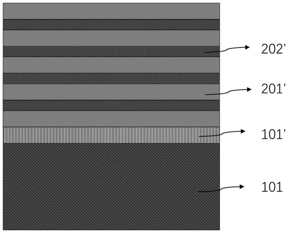
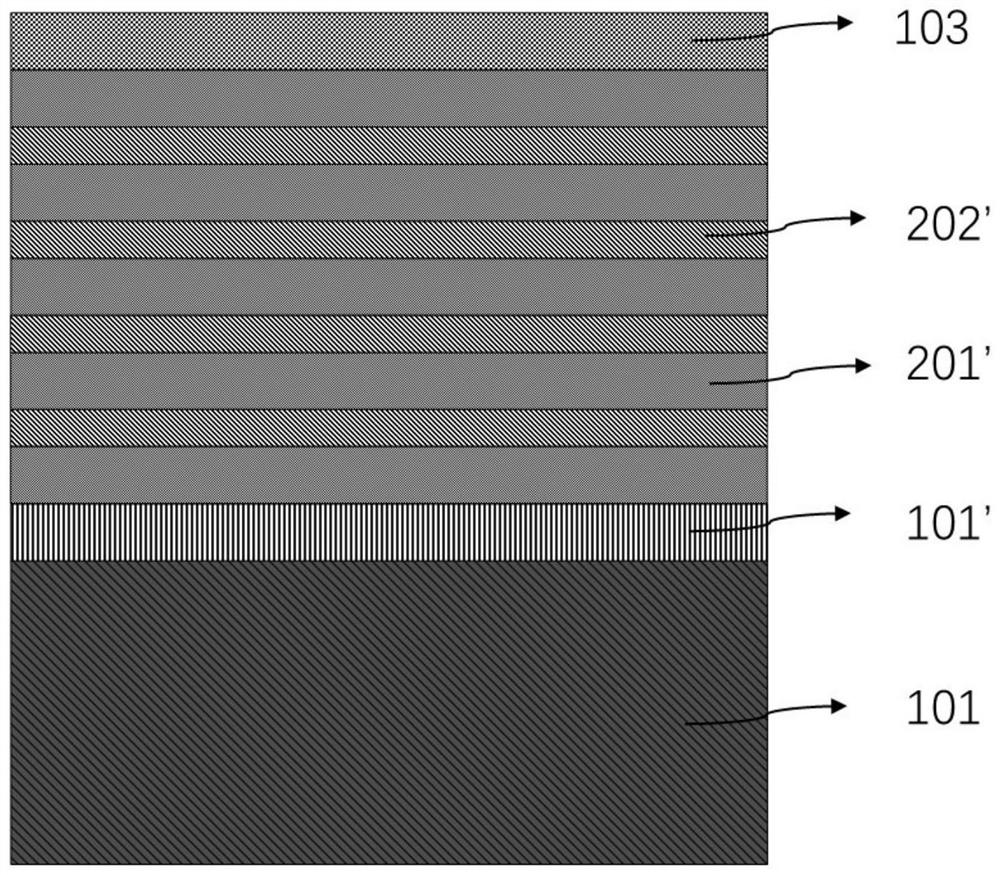
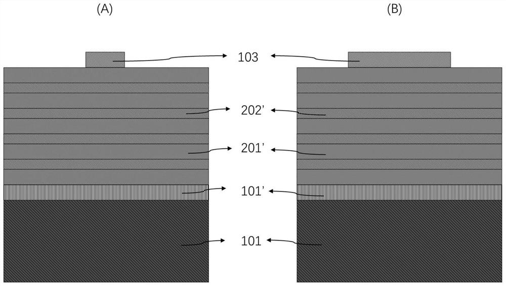
[0034] Hereinafter, embodiments of the present invention will be described with reference to the drawings. It should be understood, however, that these descriptions are exemplary only and are not intended to limit the scope of the present invention. Also, in the following description, descriptions of well-known structures and techniques are omitted to avoid unnecessarily obscuring the concept of the present invention.

[0035] Various structural schematic diagrams according to embodiments of the present invention are shown in the drawings. The figures are not drawn to scale, with certain details exaggerated and possibly omitted for clarity of presentation. The shapes of the various regions and layers shown in the figure, as well as their relative sizes and positional relationships are only exemplary, and may deviate due to manufacturing tolerances or technical limitations in practice, and those skilled in the art will Regions / layers with different shapes, sizes, and relative...


PUM

PropertyMeasurementUnit
Widthaaaaaaaaaa
Thicknessaaaaaaaaaa
Thickness rangeaaaaaaaaaa

Abstract

The invention relates to an oxide semiconductor device which includes an insulating substrate; a source electrode and a drain electrode are oppositely arranged on the insulating substrate; a nanosheet stack part is included and is arranged on the substrate to form a plurality of conducting channels; the nanosheet stack part comprises a plurality of metal oxide semiconductor nanosheets which are vertically stacked to form the nanosheet stack part, and the two ends of the metal oxide semiconductor nanosheets are embedded into the source electrode and the drain electrode respectively; and a surrounding type grid electrode is included and surrounds the periphery of the plurality of metal oxide semiconductor nanosheets in the nanometer stack part. The design of the novel structure gate-all-around OS-TFT (GAA OS-TFT) can significantly improve the sub-threshold characteristic, the current switch ratio and the short channel effect of the device; the working current of the device can be obviously improved by utilizing the design of combining the multiple layers of nanosheets and the supporting structure; the preparation process of the device is compatible with a mainstream CMOS process and is simple; and through the structure design of the surrounding type grid device, the channel carrier mobility can be remarkably improved, the electrical performance of the device is increased, and the reliability and the stability of the device can also be improved.

Description

technical field [0001] The invention relates to the field of semiconductors, in particular to an oxide semiconductor device and a preparation method thereof. Background technique [0002] Oxide thin-film transistor (English: oxide thin-film transistor (TFT)) is a special type of field effect transistor. This technology deposits the semiconductor active layer and dielectric layer in the form of a thin film on the substrate. [0003] The main difference between oxide thin film transistors and amorphous silicon thin film transistors is that the material of the electron channel is oxide instead of amorphous silicon. A commonly used substrate is silicon dioxide. Thin film transistors are mainly used in liquid crystal displays (LCDs) and organic light emitting semiconductors (OLEDs). In conventional transistors, the semiconductor material is the substrate, such as a wafer. [0004] Thin film transistor (thin film transistor, TFT) is the core device of flat panel display, whethe...

Claims


Application Information

Patent Timeline
IPC IPC(8): H01L29/786H01L29/423H01L21/34B82Y10/00B82Y40/00
CPCH01L29/78645H01L29/78696H01L29/7869H01L29/42376H01L29/66969B82Y10/00B82Y40/00
Inventor 颜刚平许高博殷华湘周娜胡艳鹏刘卫兵高建峰毕津顺
Owner INST OF MICROELECTRONICS CHINESE ACAD OF SCI
Why Eureka
Try Eureka