Molybdenum disulfide photoelectric detector and preparation method thereof

A technology of photodetectors and molybdenum disulfide, applied in circuits, electrical components, semiconductor devices, etc., can solve the problems of low photoresponse efficiency and achieve the effect of enhancing photoresponse and breaking symmetry

Pending Publication Date: 2021-10-19
深圳网联光仪科技有限公司
View PDF5 Cites 1 Cited by
  • Summary
  • Abstract
  • Description
  • Claims
  • Application Information

AI Technical Summary

Problems solved by technology

[0005] The invention provides a molybdenum disulfide photodetector and a preparation method thereof, ai

Method used


Image

  • Molybdenum disulfide photoelectric detector and preparation method thereof
  • Molybdenum disulfide photoelectric detector and preparation method thereof
  • Molybdenum disulfide photoelectric detector and preparation method thereof

Examples


preparation example Construction

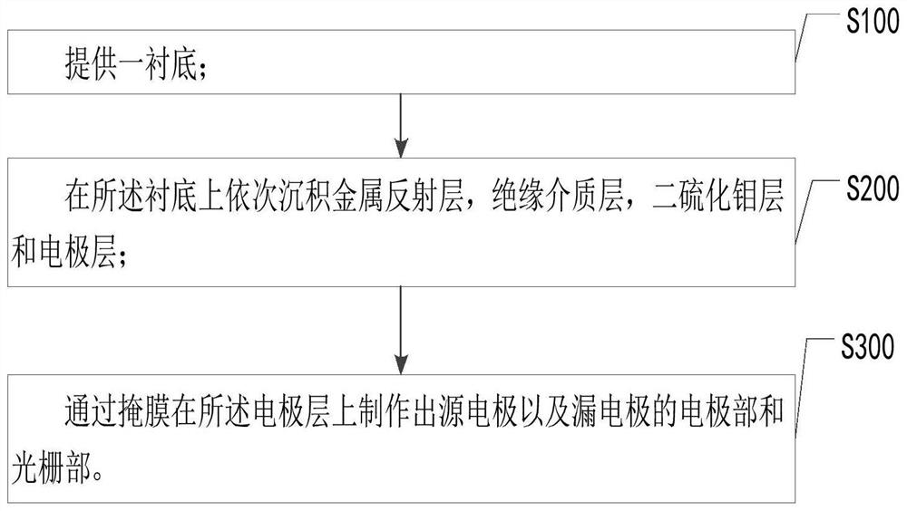
[0037] see figure 2 , the second aspect of the present invention provides a method for preparing a molybdenum disulfide photodetector, comprising:

[0038] S100, providing a substrate;

[0039]S200, sequentially depositing a metal reflective layer, an insulating dielectric layer, a molybdenum disulfide layer and an electrode layer on the substrate;

[0040] S300, fabricating the electrode part and the grating part of the source electrode and the drain electrode on the electrode layer through a mask.

[0041] The molybdenum disulfide photodetector of the present invention is integrated with molybdenum disulfide through a metamaterial optical antenna, and utilizes plasmon resonance to realize the field of the local tangential photon mode (the electric field is mainly parallel to the two-dimensional plane of molybdenum disulfide) enhanced. Based on the matching of the tangential photon mode and the light absorption direction of molybdenum disulfide, the equivalent absorption ...

Embodiment 1

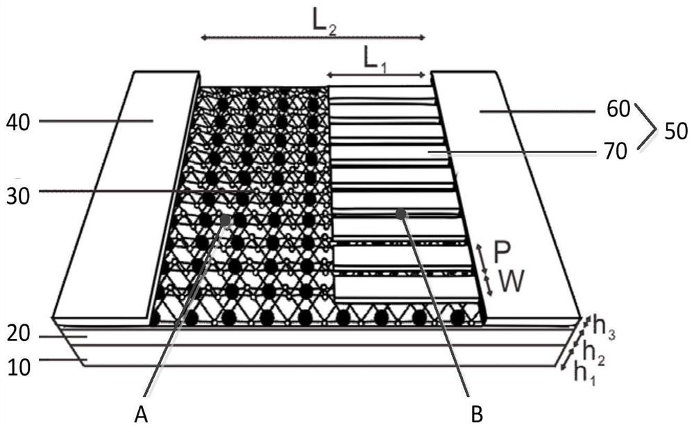
[0043] The concrete structure of a kind of molybdenum disulfide photodetector of the present invention is as follows:

[0044] The structure of the molybdenum disulfide photodetector includes: a source electrode, a drain electrode integrated with a grating, a single molybdenum disulfide layer, an insulating medium layer, and a metal reflection layer. see figure 1 , the source electrode and the drain electrode integrated with the grating are a layer of thickness h 3 A highly conductive metal whose thickness h 3 Not less than twice the skin depth of the electromagnetic wave in the metal, passing through the grid period P, the grid line width W, and the grid length L 1 and channel length L 2 The structure of the source and drain electrodes can be determined, such as L 1 equal to L 2 / 2, P is one-tenth to one-twentieth of the light wavelength, W is three-quarters of P, and the insulating dielectric layer is a layer with a thickness of h 2 transparent medium in the working ba...

Embodiment 2

[0052] The specific preparation method of a kind of molybdenum disulfide photodetector of the present invention is as follows:

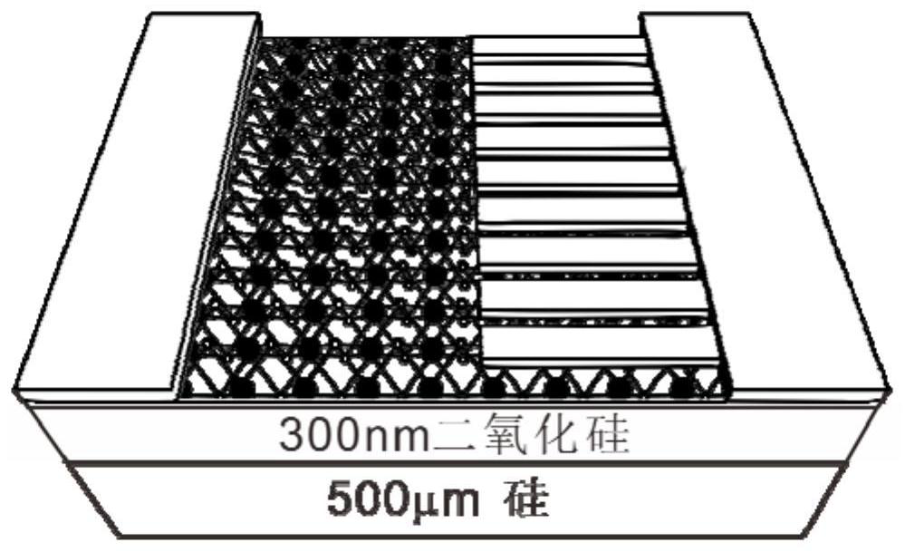
[0053] 1. First use acetone to ultrasonically clean the silicon wafer substrate, then rinse the surface of the silicon wafer with isopropanol to remove excess acetone, then rinse the silicon wafer with deionized water, dry it to ensure that the surface of the silicon wafer substrate is clean and pollution-free .

[0054] 2. On a clean silicon wafer substrate, a Ti (10nm) / Ag (100nm) metal layer is deposited as a bottom metal reflective layer by means of electron beam evaporation.

[0055] 3. Using plasma enhanced atomic layer deposition (PEALD) to deposit a layer of insulating medium transparent to the working band on the bottom metal reflective layer with a specific thickness.

[0056] 4. Transfer the monolayer molybdenum disulfide to the surface of the insulating dielectric layer by using a mechanical stripping method.

[0057] 5. Use electron bea...


PUM


Abstract

The invention provides a molybdenum disulfide photoelectric detector and a preparation method thereof. The molybdenum disulfide photoelectric detector comprises a metal reflecting layer, an insulating medium layer, a molybdenum disulfide layer, a source electrode and a drain electrode, wherein the metal reflecting layer, the insulating medium layer and the molybdenum disulfide layer are arranged from bottom to top, the source electrode and the drain electrode are arranged on the molybdenum disulfide layer at an interval, and the drain electrode comprises an electrode part and a grating part. According to the molybdenum disulfide photoelectric detector, the metal emission layer is adopted as the bottom layer, and the grating is integrated on the drain electrode, so that obvious light absorption difference can be formed between the drain electrode and the source electrode of the photoelectric detector, the symmetry of the light current at the two ends of the drain electrode and the source electrode is broken, and the light response of the photoelectric detector is enhanced.

Description

technical field [0001] The invention relates to the technical field of semiconductor sensors, in particular to a molybdenum disulfide photodetector and a preparation method thereof. Background technique [0002] Semiconductor photodetectors have long been maturely used in a wide range of fields and have become one of the core device categories of modern industry and science. At present, new two-dimensional semiconductor materials are constantly being explored and discovered because of their unique characteristics compared to traditional semiconductor materials. The physical and chemical properties of photodetection can meet the high performance requirements of photodetection in various complex scenarios at the practical application level, and it has gradually become the focus of research on cutting-edge photodetection technology. Few-layer molybdenum disulfide exhibits excellent performance in electronics and optics due to its adjustable bandgap width, atomic thickness, and ...

Claims


Application Information

Patent Timeline
IPC IPC(8): H01L31/0216H01L31/0232H01L31/113H01L31/18
CPCH01L31/02161H01L31/02327H01L31/1136H01L31/18Y02P70/50
Inventor 李浩文夏国强
Owner 深圳网联光仪科技有限公司
Why Eureka
Try Eureka