Composition for packaging optoelectronic device and packaging structure formed by composition
A technology for optoelectronic devices and compositions, which is applied in the direction of electric solid devices, electrical components, semiconductor devices, etc., can solve the problems of reducing the service life of OLED devices, reducing the luminous efficiency of OLED devices, and enhancing them, so as to achieve improved heat resistance, good sprayability, etc. Ink printing performance, the effect of preventing optical corrosion
- Summary
- Abstract
- Description
- Claims
- Application Information
AI Technical Summary
Problems solved by technology
Method used
Image

Examples
Embodiment 1
[0078] Embodiment 1: Preparation of Encapsulation Composition 1
[0079] The components used are described below:
[0080] (A) Multi-component acrylate monomer: 0.5% of 3-[3-tert-butyl-5-(5-chlorobenzothiazol-2-yl)-4-hydroxyphenyl]-2-propyl methacrylate;
[0081] (B) Multi-component acrylate monomer: 40% of pentaerythritol triacrylate;
[0082] (C) Multi-component acrylate monomer: 29.5% of 3-propyl tri(trimethoxy silicon) methacrylate;
[0083] (D) monofunctional acrylate monomer: 25% of tert-butyl acrylate;
[0084] (E) Photoinitiator: (2,4,6-trimethylbenzoyl)diphenylphosphine oxide 5%.
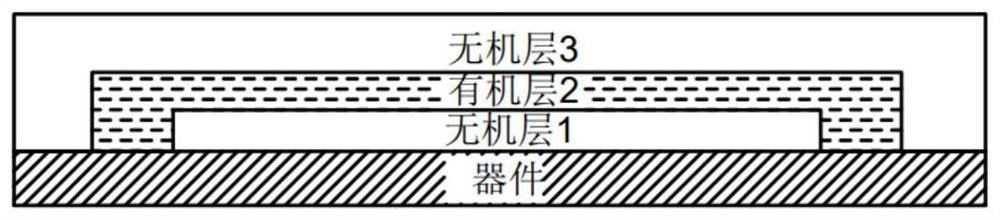
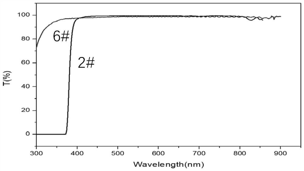
[0085] In a brown glass bottle, add 0.5% (A), 40% (B), 29.5% (C), 25% (D) and 5% (E) of the total mass, shake and mix at room temperature for 2 hours, and then filter to obtain Composition 1 for packaging; then the composition is coated on the surface of the ITO substrate by inkjet printing to form a sample with an area size of 10cm × 10cm × 10 μm (length × width × thickness), and then ...
Embodiment 2
[0095] Embodiment 2: Preparation of encapsulation composition 2
[0096] (A) Multi-component acrylate monomer: 2.5% of 3-[3-tert-butyl-5-(5-chlorobenzothiazol-2-yl)-4-hydroxyphenyl]-2-propyl methacrylate;
[0097] (B) Multi-component acrylate monomer: 40% of pentaerythritol triacrylate;
[0098] (C) Multi-component acrylate monomer: 48.5% of 3-propyl tri(trimethoxy silicon) methacrylate;
[0099] (D) Monofunctional acrylate monomer: 6% of tert-butyl acrylate;
[0100] (E) Photoinitiator: (2,4,6-trimethylbenzoyl)diphenylphosphine oxide 3%.
[0101] In a brown glass bottle, add the above raw materials, shake and mix at room temperature for 2 hours, and then filter to obtain composition 2 for packaging; then apply the composition on the surface of an ITO substrate by inkjet printing to form an area of 10cm×10cm×10μm (length×width×thickness) sample, then pass through 100mW / cm 2 The UV curing equipment cures the packaging composition by ultraviolet curing for 10 to 30 seconds...
Embodiment 3
[0102] Embodiment 3: Preparation of encapsulation composition 3
[0103](A) Polyacrylate monomer: 3-[3-tert-butyl-5-(5-chlorobenzothiazol-2-yl)-4-hydroxyphenyl]-2-propyl methacrylate 9%;
[0104] (B) Multi-component acrylate monomer: 20% of pentaerythritol triacrylate;
[0105] (C) Multi-component acrylate monomer: 20% of 3-methacrylic acid propyl tri(trimethoxy silicon);
[0106] (D) monofunctional acrylate monomer: 50% of tert-butyl acrylate;
[0107] (E) Photoinitiator: (2,4,6-trimethylbenzoyl)diphenylphosphine oxide 1%.
[0108] In a brown glass bottle, add the above raw materials, shake and mix at room temperature for 2 hours, and then filter to obtain the composition 3 for packaging; then apply the composition on the surface of the ITO substrate by inkjet printing to form an area of 10cm×10cm×10μm (length×width×thickness) sample, then pass through 100mW / cm 2 UV curing equipment UV curing for 10 to 30 seconds to cure the packaging composition, and finally form a pac...
PUM
 Abstract
Description
Claims
Application Information
 - R&D
- Intellectual Property
- Life Sciences
- Materials
- Tech Scout
- Unparalleled Data Quality
- Higher Quality Content
- 60% Fewer Hallucinations
Browse by: Latest US Patents, China's latest patents, Technical Efficacy Thesaurus, Application Domain, Technology Topic, Popular Technical Reports.
© 2025 PatSnap. All rights reserved.Legal|Privacy policy|Modern Slavery Act Transparency Statement|Sitemap|About US| Contact US: help@patsnap.com