Thinned crystalline silicon cell and preparation method thereof
A crystalline silicon cell and thinning technology, applied in circuits, photovoltaic power generation, electrical components, etc., can solve the problems of immature thin crystalline silicon cell preparation technology, decreased cell conversion efficiency, and reduced crystalline silicon cell thickness, etc. Absorption and efficiency loss, improved conversion efficiency, cost-effective effect
- Summary
- Abstract
- Description
- Claims
- Application Information
AI Technical Summary
Problems solved by technology
Method used
Image
Examples
Embodiment 1
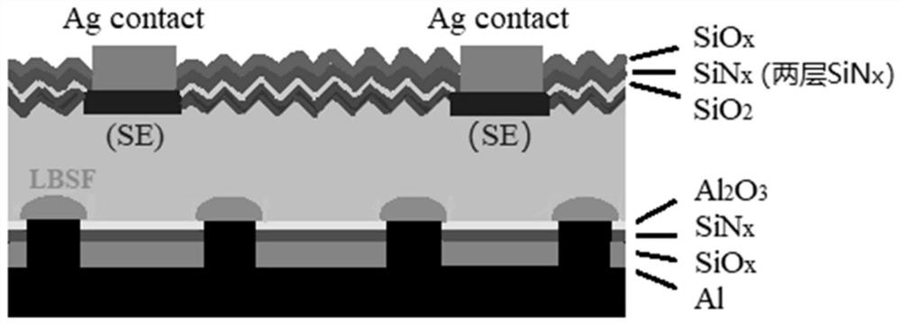
[0025] Embodiment one, such as figure 1 Shown:
[0026] Step 1: Al is sequentially prepared on the back of a p-type single crystal silicon wafer with a thickness of 100 microns 2 o 3 thin film, third SiN x Thin film and second SiO x thin film; the Al 2 o 3 film thickness of 8 nm, the third SiN x The film thickness is 30 nm, the second SiO x The thickness of the film is 200 nm;
[0027] Step 2: Laser drilling is used on the back of the p-type single crystal silicon wafer obtained in step 1, and a p+ local back surface field is formed in the hole, and an aluminum electrode is formed by screen printing; the substrate resistivity of the p-type single crystal silicon wafer is 0.9Ωcm.
[0028] Step 3: Texturing the upper surface of the product obtained in Step 2 to form randomly distributed pyramids with a characteristic size of 1-2um;
[0029] Step 4: On the product obtained in Step 3, use POCl at a temperature of 840°C 3 The diffusion method forms the n+ emitter to obta...
Embodiment 2
[0039] Step 1: Al is sequentially prepared on the back of a p-type single crystal silicon wafer with a thickness of 120 microns 2 o 3 thin film, third SiN x Thin film and second SiO x thin film; the Al 2 o 3 film thickness of 10 nm, the third SiN x The film thickness is 38 nm, the second SiO x The film thickness is 220 nm;
[0040] Step 2: Drill holes on the back of the p-type single crystal silicon wafer obtained in step 1, and form a p+ local back surface field in the holes, and form aluminum electrodes by screen printing;
[0041] Step 3: Texturing the upper surface of the product obtained in Step 2 to form randomly distributed pyramids with a characteristic size of 1-2um;
[0042] Step 4: On the product obtained in Step 3, use POCl at a temperature of 880°C 3 The diffusion method forms the n+ emitter to obtain a p-n junction, wherein the doping concentration of the n+ emitter is 1.2×10 19 / cm 3 ;
[0043] Step 5: SiO is sequentially prepared on the upper surface...
Embodiment 3
[0046] A method for preparing a thinned crystalline silicon battery, the method specifically comprising the following steps:
[0047] Step 1: Al is sequentially prepared on the back of a p-type single crystal silicon wafer with a thickness of 140 microns 2 o 3 thin film, third SiN x Thin film and second SiO x thin film; the Al 2 o 3 film thickness of 15 nm, a third SiN x The film thickness is 45 nm, the second SiO x The film thickness is 250 nm;
[0048] Step 2: Drill holes on the back of the p-type single crystal silicon wafer obtained in step 1, and form a p+ local back surface field in the holes, and form aluminum electrodes by screen printing;
[0049] Step 3: Texturing the upper surface of the product obtained in Step 2 to form randomly distributed pyramids with a characteristic size of 1-2um;
[0050] Step 4: On the product obtained in Step 3, use POCl at a temperature of 900°C 3 The diffusion method forms the n+ emitter to obtain a p-n junction, wherein the dop...
PUM
| Property | Measurement | Unit |
|---|---|---|
| thickness | aaaaa | aaaaa |
| thickness | aaaaa | aaaaa |
| thickness | aaaaa | aaaaa |
Abstract
Description
Claims
Application Information


