Tunable mode converter and preparation method thereof

A mode converter and device technology, applied in the direction of optical waveguide light guide, optics, light guide, etc., can solve the problems of small number of modes, limited optical communication data transmission capacity, and device inability to tune, and achieve low production cost, strong interference effect, The effect of large thermo-optic coefficient

Active Publication Date: 2021-11-09
JILIN UNIV
View PDF11 Cites 4 Cited by
  • Summary
  • Abstract
  • Description
  • Claims
  • Application Information

AI Technical Summary

Problems solved by technology

[0005] However, the number of modes that can be converted by traditional mode converters is relatively small, and most devices cannot be tuned, which limits the further improvement of optical communication data transmission capacity.

Method used


Image

  • Tunable mode converter and preparation method thereof
  • Tunable mode converter and preparation method thereof
  • Tunable mode converter and preparation method thereof

Examples


Embodiment 1

[0071] The present invention will be further described below in conjunction with drawings and embodiments.

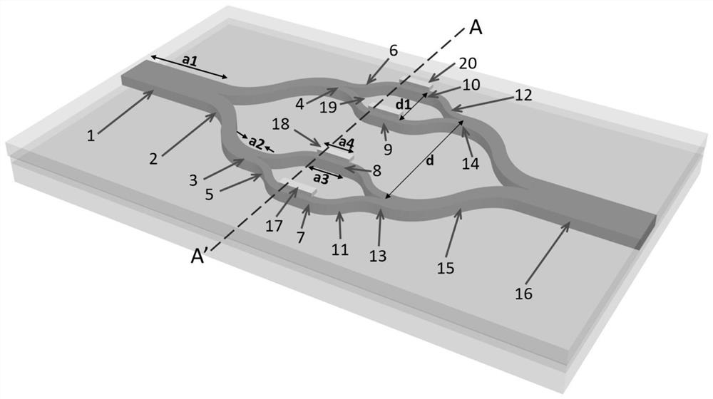
[0072] Example structure such as figure 1 As shown, the lengths a1 and a1' of the input few-mode straight waveguide 1 and the output few-mode straight waveguide 16 are equal to 1 cm, the first input straight waveguide 3, the second input straight waveguide 4, the first output straight waveguide 13, the second output straight waveguide The lengths a2, a2', a2", a2"' of the straight waveguide 14 are equal to 500 μm. The lengths a3, a3', a3", a3"' of the first modulation arm 7, the second modulation arm 8, the third modulation arm 9 and the fourth modulation arm 10 are equal to 0.3cm, and the two parallel MZI optical waveguide structures The center distance d between the interference arms is 104 μm, the center distance d1 between the two parallel interference arms of the secondary MZI optical waveguide structure is equal to 52 μm, the first heating electrode 17, the secon...

Embodiment 2

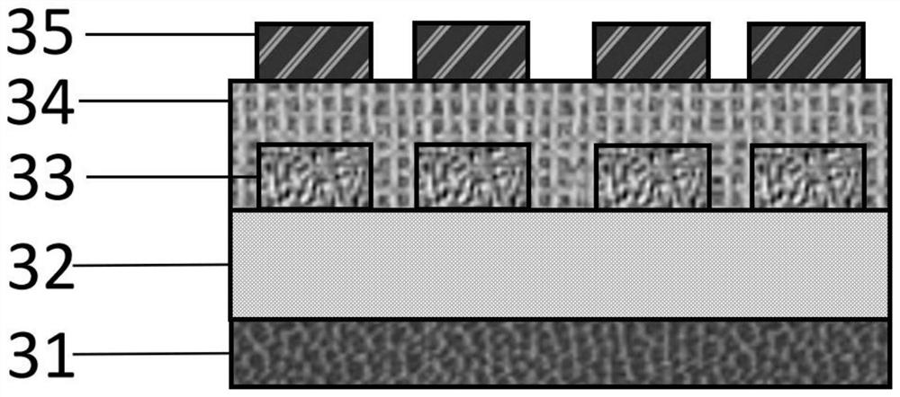
[0094] Cleaning of the silicon wafer substrate: Wipe the silicon wafer substrate repeatedly with a cotton ball dipped in acetone, then repeatedly wipe the silicon wafer substrate with a cotton ball dipped in ethanol, then rinse it with deionized water, and dry it with nitrogen Place into a clean Petri dish and seal.

[0095] Preparing the lower cladding layer 32 of silicon dioxide by thermal oxidation: growing a lower cladding layer of silicon dioxide with a thickness of 15 μm by thermal oxidation.

[0096] The optical waveguide core layer 33 of the device including the input / output region, Y branch beam splitter / coupler and modulation arm is prepared by spin coating, photolithography, and wet etching processes: the spin coating process will have a negative thermo-optic coefficient The polymer material SU-82002 is spin-coated on the clean silicon dioxide lower cladding layer at a speed of 2500 rpm, and the silicon wafer spin-coated with the polymer film is pre-baked, and the t...


PUM

PropertyMeasurementUnit
thicknessaaaaaaaaaa
thicknessaaaaaaaaaa
thicknessaaaaaaaaaa

Abstract

The invention discloses a tunable mode converter and a manufacturing method thereof, and belongs to the technical field of planar optical waveguide devices. The tunable mode converter is based on an MZI optical waveguide structure. Along the propagation direction of light, the tunable mode converter is formed by an input few-mode straight waveguide, a 3-dBY branch beam splitter, a first input straight waveguide, a second input straight waveguide, a first 3-dBY branch beam splitter, a second 3-dBY branch beam splitter, four modulation arms, a first 3-dBY branch coupler, a second 3-dBY branch coupler, a first output straight waveguide, a second output straight waveguide, a 3-dBY branch coupler, an output few-mode straight waveguide and four parallel heating electrodes. The tunable mode converter comprises a silicon wafer substrate, a silicon dioxide lower cladding, an optical waveguide core layer with a strip-shaped structure and a polymer upper cladding 34 structure from bottom to top. The heating electrode is located right above the modulation arm, and the refractive index of the core layer material is higher than that of the upper cladding layer material. According to the invention, the modulation arm of the MZI structure is modulated to realize the purpose of mutual conversion of four optical modes.

Description

technical field [0001] The invention belongs to the technical field of planar optical waveguide devices, and in particular relates to an optical waveguide core layer and an upper cladding layer with silicon wafer as a substrate, silicon dioxide as a lower cladding layer, and an organic polymer material with a high thermo-optic coefficient. Tunable mode converter and its preparation method. Background technique [0002] With the rapid development of Internet technology, the amount of data to be transmitted is increasing exponentially. The traditional electrical interconnection has been difficult to meet the demand for rapidly increasing data transmission. Therefore, optical interconnection has emerged as the times require. Different from the traditional electrical interconnection, the optical interconnection uses light as the medium of data transmission, which greatly improves the data transmission speed. Traditional single-mode fiber can only transmit one mode of light. In ...

Claims


Application Information

Patent Timeline
Patent Type & Authority Applications(China)
IPC IPC(8): G02B6/12
CPCG02B6/12G02B2006/12152G02B2006/12069
Inventor 王希斌孙士杰林柏竹杨凯迪朱穆张大明
Owner JILIN UNIV
Why Eureka
Try Eureka