Black phosphorus thin film reaction device, black phosphorus thin film preparation method

A reaction device and thin film technology, applied in the field of two-dimensional materials, can solve the problems of high pressure, low crystal quality, and difficulty in controlling nucleation points, and achieve the effect of inhibiting the formation of nucleation points and improving uniformity

Active Publication Date: 2022-01-07
SUZHOU INST OF NANO TECH & NANO BIONICS CHINESE ACEDEMY OF SCI
View PDF0 Cites 0 Cited by
  • Summary
  • Abstract
  • Description
  • Claims
  • Application Information

AI Technical Summary

Problems solved by technology

[0003] Although black phosphorus has great application prospects, the current research progress on the epitaxial growth of its thin films still faces many problems, which hinder the large-scale application of black phosphorus materials in the field of devices.
At present, there are mainly two methods for the preparation of black phosphorus thin films: chemical vapor transport method and laser pulse deposition method. The existing two methods cannot obtain single crystal thin films with high crystal quality.
[0004] For the existing chemical vapor transport method, the reactant and the growth substrate are placed in the same cavity, and under a certain temperature and pressure, nucleation is induced on the substrate by the action of a mineralizer, and then a black phosphorus film is grown. , during the heat treatment process, the pressure of the reactants and the growth substrate is the same, and the existing problems include at least: the pressure required to meet the black phosphorus phase transformation nuclear epitaxy is relatively high, and it is difficult to control the formation of nucleation sites under such a large pressure , it is easy to get a lot of nucleation sites to grow at the same time, so as to finally get polycrystalline films with low crystalline quality, and it is difficult to extend this technology to the growth of high-quality black arsenic-phosphorus alloy films

Method used


Image

  • Black phosphorus thin film reaction device, black phosphorus thin film preparation method
  • Black phosphorus thin film reaction device, black phosphorus thin film preparation method
  • Black phosphorus thin film reaction device, black phosphorus thin film preparation method

Examples


preparation example Construction

[0046] According to a method for preparing a black phosphorus film according to a preferred embodiment of the present invention, the method includes:

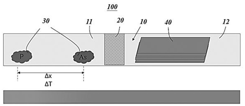
[0047] s1, provide figure 1 The black phosphorus thin film reaction device 100;

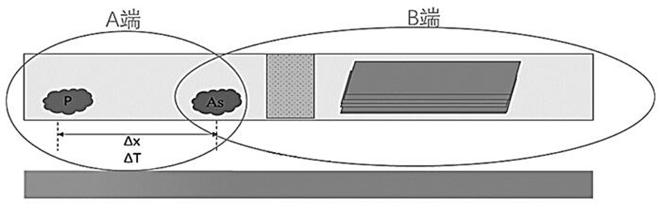
[0048] s2, placing the reactant 30 and the growth substrate 40 in the first reaction chamber 11 and the second reaction chamber 12, respectively, where the reactant 30 at least includes a phosphorus source and a mineralizer;

[0049] Heating causes the phosphorus-containing gas to enter the second reaction chamber 12 from the first reaction chamber 11 , and forms a black phosphorus film on the surface of the growth substrate 40 .

[0050]In some embodiments, the reactant further includes an arsenic source, the phosphorus source and the arsenic source are located at different positions in the first reaction chamber, and the temperature at the position of the arsenic source is controlled to be greater than the temperature at the position of the pho...

Embodiment 1

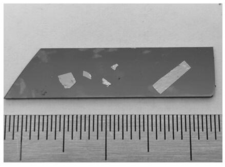
[0063] Example 1: Preparation of Black Phosphorus Single Crystal Thin Film

[0064] Preparation of reaction apparatus and raw materials:

[0065] Provide 5 pieces of Si / SiO evaporated with 5nm-150nm thickness of Au metal film 2 sheet as a substrate for thin film growth. And provide red phosphorus, tin tetraiodide and tin particles as raw materials, the quality of these raw materials are 50mg, 5mg and 10mg respectively.

[0066] supply figure 1 The black phosphorus thin film reaction device shown uses a straight quartz tube as the reaction chamber. In the middle of the reaction chamber, there is a columnar buffer section filled with silicon oxide particles. This section divides the reaction chamber into two parts that communicate with each other through the silicon oxide particles. The raw material is placed in one section of the reaction chamber, and the silicon wafers coated with gold layer are stacked and placed in the other section of the reaction chamber.

[0067] Grow...

Embodiment 2

[0069] Example 2: Preparation of Black Phosphorus Single Crystal Thin Film

[0070] Preparation of reaction apparatus and raw materials:

[0071] Provide 4 pieces of Si / SiO deposited with 5nm-150nm thickness gold film 2 sheet as a substrate for thin film growth. And provide red phosphorus, iodine and tin particles as raw materials, the mass of these raw materials are 150mg, 5mg and 50mg respectively.

[0072] supply figure 1 The black phosphorus thin film reaction device shown uses a straight quartz tube as the reaction chamber. There is a quartz column in the middle of the reaction chamber, and a capillary channel with a diameter of 0.3 mm exists in the quartz column. This section of quartz column divides the reaction chamber into each other and passes through each other. The two connected sections of the capillary channel, the raw material is placed in one section of the reaction chamber, and the silicon wafers plated with gold layer are stacked and placed in the other se...


PUM

PropertyMeasurementUnit
particle diameteraaaaaaaaaa
sizeaaaaaaaaaa

Abstract

The invention discloses a black phosphorus film reaction device and a method for preparing a black phosphorus film. The device includes a vacuum-tight reaction chamber, and a slow-release body is arranged in the reaction chamber, and the slow-release body separates the reaction chamber A first reaction chamber for placing reactants and a second reaction chamber for placing growth substrates, capillary channels are formed in the sustained-release body, and the pressure in the second reaction chamber is controlled to be lower than that of the first reaction chamber during the heated reaction process. pressure in the cavity. In the present invention, a section of slow-release material is set between the reactant and the growth substrate to moderately suppress the transmission of the gaseous source in the first reaction chamber to the second reaction chamber, thereby controlling the pressure at the growth end from being too high, that is, the second The pressure of the reaction chamber is lower than the pressure of the first reaction chamber, which improves the uniformity of source supply over time, effectively suppresses the formation of excessive nucleation points on the substrate, and finally obtains a high-quality single crystal film or alloy film.

Description

technical field [0001] The invention relates to the technical field of two-dimensional materials, in particular to a black phosphorus thin film reaction device and a method for preparing the black phosphorus thin film. Background technique [0002] In recent years, as a direct-bandgap two-dimensional semiconductor material, black phosphorus has received extensive attention in electronic and optoelectronic applications due to its narrow bandgap characteristics and tunable direct bandgap. In addition, using the alloying strategy to substitute arsenic atoms into black phosphorus crystals can form a black arsenic phosphorus alloy, which can realize the band gap adjustment of the black phosphorus material system and further enhance the competition of the black phosphorus material system in the fields of optoelectronic devices and other fields. Advantage. [0003] Although black phosphorus has great application prospects, the current research progress on the epitaxial growth of i...

Claims


Application Information

Patent Timeline
Patent Type & Authority Patents(China)
IPC IPC(8): C30B29/02C30B25/16C30B25/14
CPCC30B29/02C30B25/165C30B25/14
Inventor 张凯陈程陈捷
Owner SUZHOU INST OF NANO TECH & NANO BIONICS CHINESE ACEDEMY OF SCI
Why Eureka
Try Eureka