
Copper-based surface-enhanced Raman scattering substrate as well as preparation method and application thereof

A Raman scattering-based, surface-enhancing technology, applied in Raman scattering, sputtering plating, ion implantation plating, etc., can solve the problems of general enhancement effect, limited application, inconvenient storage, etc., and achieve enhanced enhancement effect , storage, and convenient use

Active Publication Date: 2021-11-19
TSINGHUA UNIV
View PDF6 Cites 0 Cited by
  • Summary
  • Abstract
  • Description
  • Claims
  • Application Information

AI Technical Summary

Problems solved by technology

[0005] The object of the present invention is to provide a copper-based surface-enhanced Raman scattering substrate and its preparation method and application, so as to solve the problem of silicon wafer or glass in the prior art When other hard materials are used as the substrate, there are problems such as cutting, inconvenient storage, general enhancement effect, and limited application.

Method used


Image

  • Copper-based surface-enhanced Raman scattering substrate as well as preparation method and application thereof
  • Copper-based surface-enhanced Raman scattering substrate as well as preparation method and application thereof
  • Copper-based surface-enhanced Raman scattering substrate as well as preparation method and application thereof

Examples


preparation example Construction

[0028] A method for preparing a copper-based surface-enhanced Raman scattering substrate provided in an optional embodiment may include the following steps:

[0029] In step S1, the metal copper foil is coated with an aluminum oxide layer of a certain thickness by atomic layer deposition. Wherein, the temperature is 80° C. to 200° C., and the coating can be successful and the coating effect is better at this temperature. For example, the temperature can be set to 150° C. and the like. The coating thickness of aluminum oxide is 4nm-12nm, and the corresponding number of coating cycles is 40-120 cycles; more preferably, the number of coating cycles is 60-120 cycles, and the corresponding coating thickness of aluminum oxide is 6nm ~ 12nm. For the thickness of the metal copper foil, the inventor has found through many experiments that wrinkles are easy to occur when the thickness is less than 20 microns, and the cost will increase when the thickness is greater than 80 microns, so ...

Embodiment 1

[0034] Embodiment 1 (not coated aluminum oxide)

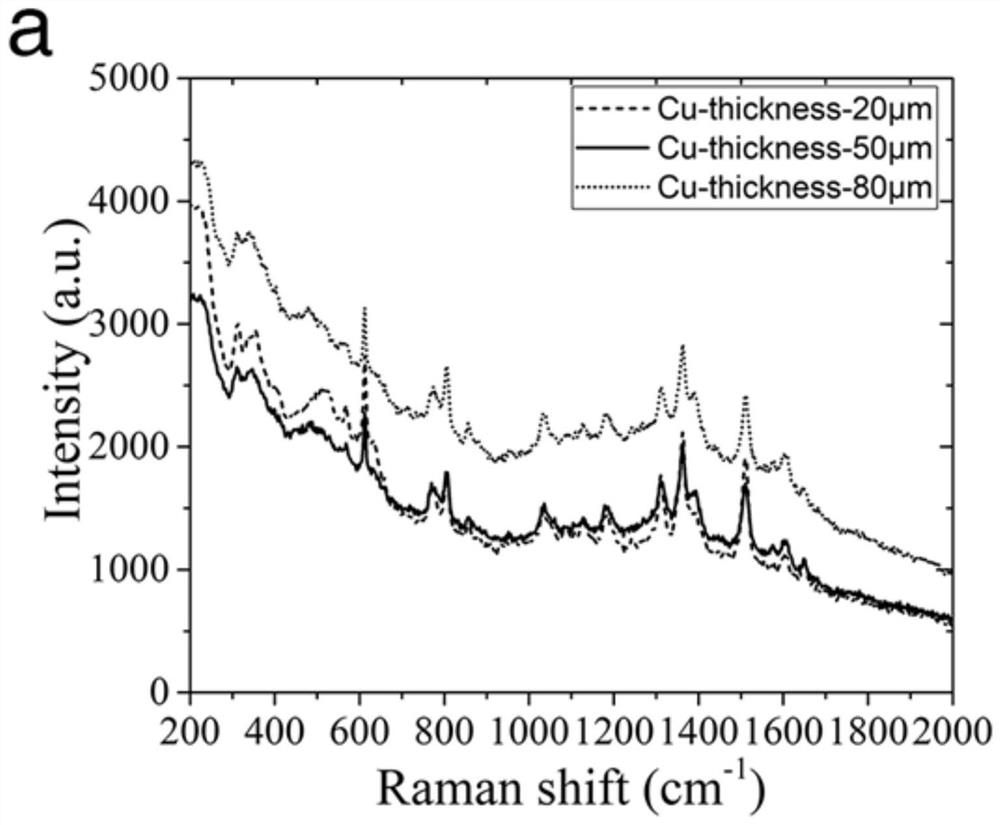
[0035] 1. Take copper foils with a thickness of 20μm, 50μm and 80μm respectively, and clean them;

[0036] 2. At room temperature, using high-purity silver as the evaporation target, pump the reaction chamber of the electron beam evaporation deposition coating machine to 5×10 -5 Pa high vacuum;

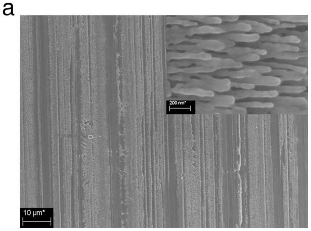
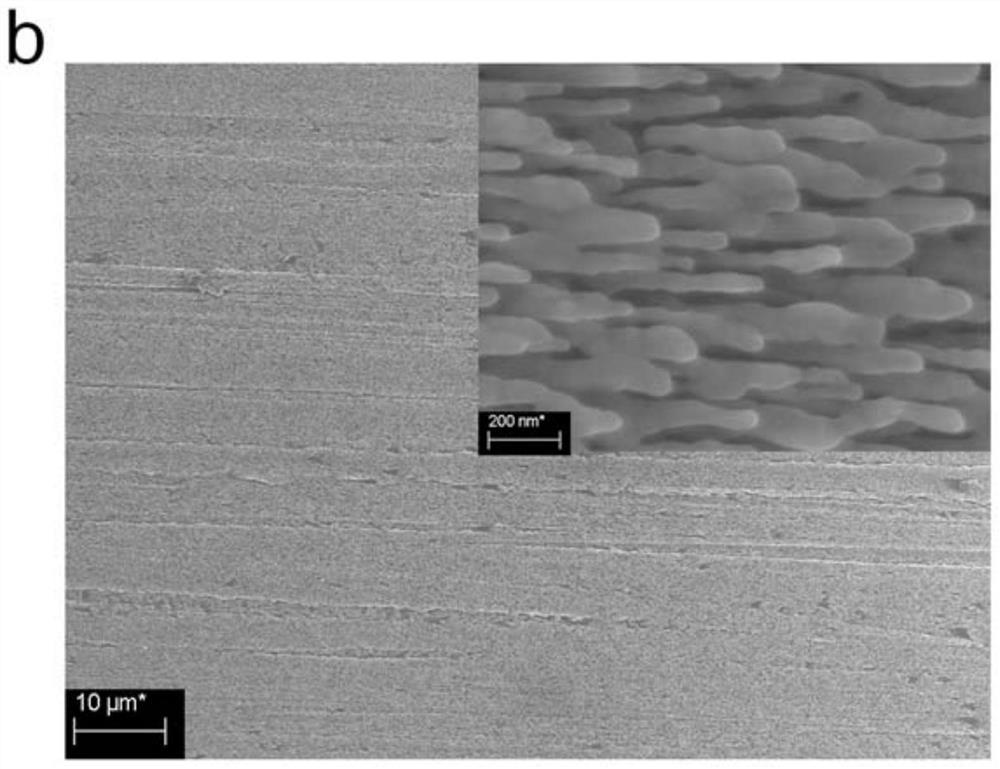
[0037] 3. Fix the copper foil flatly on the substrate stage, divide the copper foil into two groups, one group makes the copper foil scratches along the vertical direction, and the other group makes the copper foil scratches along the horizontal direction; adjust the substrate The angle of the table normal makes the included angle between the direction of the evaporation beam flow and the normal of the substrate table be 86°, and the silver nanowires with a crystal oscillator of 800 nm are grown obliquely on the substrate of the substrate table to obtain a surface-enhanced Raman scattering substrate ;

[0038] 4. Preparation 10 -5 ...

Embodiment 2

[0044] 1. Deposit 0, 40, 60, 80, 100, 120 cycles of aluminum oxide on the cleaned copper foil with a thickness of 50 μm at 150 ° C;

[0045] 2. At room temperature, using high-purity silver as the evaporation target, pump the reaction chamber of the electron beam evaporation deposition coating machine to 5×10 -5 Pa high vacuum;

[0046] 3. Fix the copper foil on the substrate table so that the scratches on the copper foil are in the vertical direction, and adjust the angle of the normal line of the substrate table so that the angle between the direction of the evaporation beam and the normal line of the substrate table is 86°. On the base of the stage, silver nanowires with a diameter of 800nm ​​are obliquely grown on the crystal oscillator to obtain a surface-enhanced Raman scattering substrate;

[0047] 4. Preparation 10 -5 The rhodamine 6G (R6G) solution of mol / L;

[0048] 5. Cut the surface-enhanced Raman scattering substrate prepared in step 3 into a 5mm square piece, ...


PUM

PropertyMeasurementUnit
thicknessaaaaaaaaaa
thicknessaaaaaaaaaa

Abstract

The invention discloses a copper-based surface-enhanced Raman scattering substrate as well as a preparation method and application thereof. The substrate comprises a copper foil substrate layer and a silver nanowire structure layer attached to the copper foil substrate layer, and the copper foil substrate layer is coated with an aluminum oxide layer. The preparation method comprises the following steps: coating a metal copper foil with aluminum oxide by adopting an atomic layer deposition method to obtain a copper foil substrate coated with aluminum oxide; and depositing metal silver on the copper foil substrate coated with the aluminum oxide along the scratch direction of the copper foil by adopting an electron beam evaporation inclined deposition method to form a silver nanowire structure. The copper-based surface-enhanced Raman scattering substrate is good in enhancement effect, has flexibility and ductility of metal copper, can be applied to rapid detection of trace or even trace organic matters, and has the advantages of being low in cost, convenient to transport and store and wide in application range.

Description

technical field [0001] The invention relates to the technical field of trace organic matter detection, in particular to a copper-based surface-enhanced Raman scattering substrate and a preparation method and application thereof. Background technique [0002] The surface-enhanced Raman scattering effect (SERS) can realize the fingerprint identification of chemical, biological and other organic molecules. At the same time, due to the high enhancement factor, it can realize the sensitive detection of trace or even trace substances in the system, with high sensitivity and fast test speed. , low cost, simple sample preparation and many other advantages. Since the intrinsic Raman scattering signal of the material is very weak, in order to realize the detection of the Raman fingerprint scattering signal of the material, gold, silver, copper and other precious metal nanostructures are often used as the surface-enhanced Raman scattering substrate to realize the amplification of the m...

Claims


Application Information

Patent Timeline
Patent Type & Authority Applications(China)
IPC IPC(8): G01N21/65C23C14/16C23C14/30C23C16/40C23C16/455C23C28/00
CPCG01N21/658C23C16/403C23C14/30C23C14/16C23C16/45527C23C28/322C23C28/345
Inventor 张政军赵丰通王炜鹏单博涵
Owner TSINGHUA UNIV
Learn More