Plasmon enhanced tellurium-cadmium-mercury microcavity infrared detector and preparation method thereof
A plasmon enhancement, infrared detector technology, applied in electrical components, semiconductor devices, final product manufacturing and other directions, to achieve the effect of improving infrared light absorption, reducing dark current, and increasing operating temperature
- Summary
- Abstract
- Description
- Claims
- Application Information
AI Technical Summary
Problems solved by technology
Method used
Image
Examples
Embodiment 1
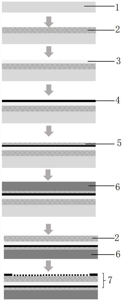
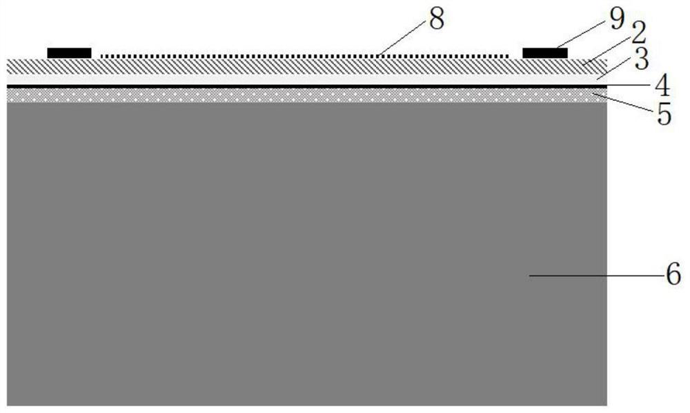
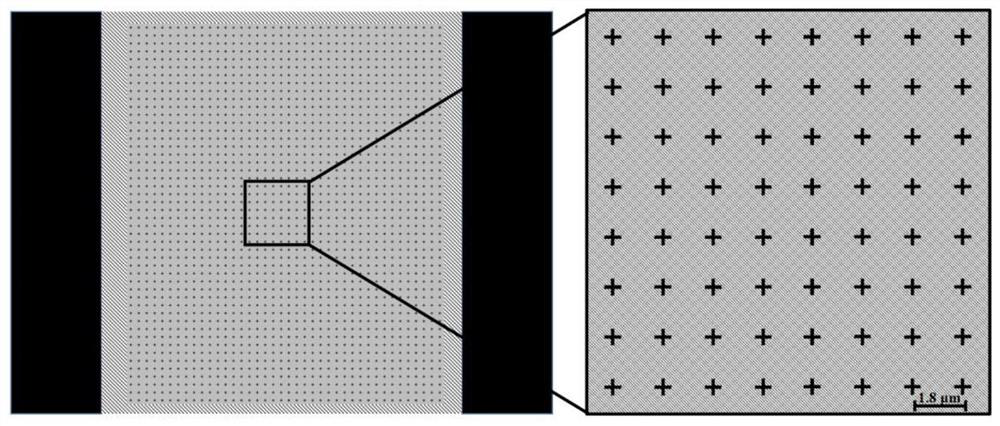
[0025] Such as figure 2 As shown, a plasmon-enhanced mercury cadmium telluride microcavity infrared detector includes silicon substrate 6, epoxy resin glue 5, gold reflective layer 4, cadmium telluride passivation layer 3, HgCdTe thin film 2, micro-nano structure 8 and electrode 9. Wherein, the thickness h of the micro-nano structure 8 1 is 60 nm, the thickness h of the metal reflective layer 2 is 120 nm, both of which are greater than the skin depth of gold by 10 nm; the thickness h of HgCdTe thin film 2 3 = 530 nm, refractive index n 3 = 3.43, the thickness h of the cadmium telluride passivation layer 3 4 = 300 nm, refractive index n 4 = 2.68; at this time, for the incident light with a detection wavelength of about 3.5 μm, n 3 h 3 +n 4 h 4 = 2621.9 ≈ 3λ / 4; the micro-nano structure 8 is a golden cross antenna array, such as image 3 As shown, the arm length of the golden cross antenna is 600 nm, the arm width is 120 nm, and the array period is 1.8 μm. The un...
Embodiment 2
[0037] Such as Figure 5 As shown, a plasmon-enhanced mercury cadmium telluride microcavity infrared detector, its structure includes silicon substrate, epoxy resin glue, gold reflective layer, 300 nm thick zinc sulfide passivation layer, 1100 nm thick HgCdTe films, micro-nano structures and electrodes. Among them, such as Figure 6 As shown, the micro-nano structure is a gold square periodic array. The gold square periodic array uses four squares with side lengths of 500 nm, 550 nm, 600 nm, and 650 nm as multiplexing structural units, and the multiplexing structural period is 3.6 μm. The unit detection area is 108 μm×129.6 μm, and the electrode size is 34 μm×34 μm. The structure and the infrared absorption spectrum of the 1100 nm thick HgCdTe thin film are as follows Figure 7 shown. The structure has a maximum photoresponsivity at a wavelength of 3.9 μm, and its dark current is reduced by more than 4 times compared with flat-film thin-film detectors with the same absorpt...
PUM
| Property | Measurement | Unit |
|---|---|---|
| thickness | aaaaa | aaaaa |
| thickness | aaaaa | aaaaa |
| thickness | aaaaa | aaaaa |
Abstract
Description
Claims
Application Information


