High-aluminum-component nitride ohmic contact device and preparation method thereof

A technology of ohmic contact and nitride, which is applied in the field of microelectronics, can solve the problems of deteriorating device dynamic characteristics, poor quality, and difficult process, so as to avoid dissociation and the introduction of surface defects, reduce contact resistivity, and improve tunneling. The effect of passing current

Pending Publication Date: 2021-12-17
XIDIAN UNIV
View PDF3 Cites 2 Cited by
  • Summary
  • Abstract
  • Description
  • Claims
  • Application Information

AI Technical Summary

Problems solved by technology

[0005] 1. Source-drain regrowth introduces an additional process, which increases the complexity of the process, and the process is difficult. Molecular Beam Epitaxy (MBE for short) or Metal-organic Chemical Vapor Deposition (Metal-organic Chemical) Vapor DePosition, referred to as MOCVD) regrowth equipment maintenance costs are high;
[0006] 2. Since ion implantation needs to activate and implant Si ions, the activation temperature is above 1000°C, which will easily cause the barrier components to dissociate, deteriorate the quality, and easily increase the defect states on the barrier surface, deteriorating the dynamic characteristics of the device

Method used


Image

  • High-aluminum-component nitride ohmic contact device and preparation method thereof
  • High-aluminum-component nitride ohmic contact device and preparation method thereof
  • High-aluminum-component nitride ohmic contact device and preparation method thereof

Examples


Embodiment Construction

[0050] The present invention will be described in further detail below in conjunction with specific examples, but the embodiments of the present invention are not limited thereto.

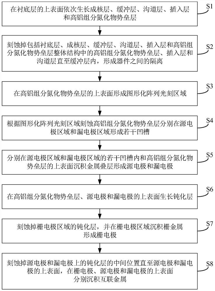
[0051] In order to still prepare an ohmic contact device with low contact resistivity on the basis of simplifying the process, in the first aspect, please refer to figure 1 , an embodiment of the present invention provides a method for preparing a high-aluminum composition nitride ohmic contact device, comprising the following steps:

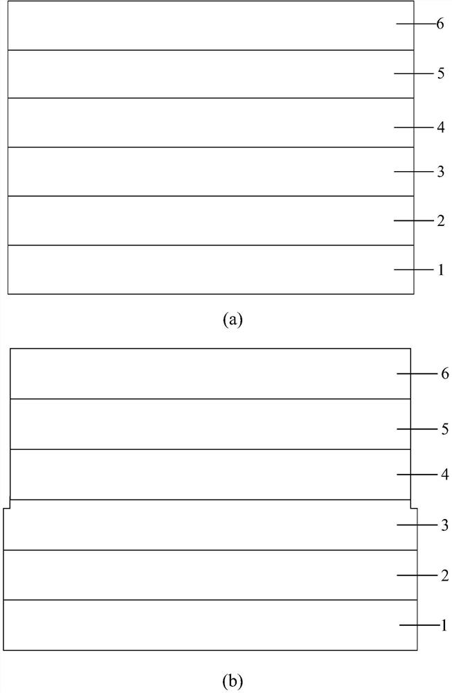
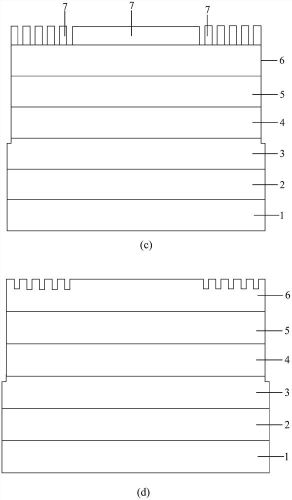
[0052] S1 , growing a nucleation layer 2 , a buffer layer 3 , a channel layer 4 , an insertion layer 5 and a nitride barrier layer 6 with a high aluminum composition in sequence on the upper surface of the substrate layer 1 .

[0053] Specifically, see figure 2 a, Step S1 of the embodiment of the present invention includes: growing an AlN nucleation layer 2 with a thickness of 50 nm to 80 nm on the upper surface of the sapphire or high-resistance Si substrate layer...


PUM

PropertyMeasurementUnit
thicknessaaaaaaaaaa
thicknessaaaaaaaaaa
thicknessaaaaaaaaaa

Abstract

The invention discloses a high-aluminum-component nitride ohmic contact device and a preparation method thereof. The preparation method comprises the following steps: sequentially growing a nucleating layer, a buffer layer, a channel layer, an insertion layer and a high-aluminum-component nitride barrier layer on a substrate layer; etching a part of the high aluminum component nitride barrier layer, a part of the insertion layer and a part of the channel layer into the buffer layer; forming a graphical array photoetching region on the high-aluminum component nitride barrier layer; etching the high-aluminum component nitride barrier layer according to the patterned array photoetching region to form a plurality of grooves; forming a source electrode and a drain electrode in the plurality of grooves of the source electrode region and the drain electrode region and the high-aluminum-component nitride barrier layer respectively; growing a passivation layer on the high-aluminum-component nitride barrier layer, the source electrode and the drain electrode; etching the passivation layer in the gate electrode region, and forming a gate electrode in the gate electrode region; and depositing interconnection metal on the gate electrode, the source electrode and the drain electrode respectively. The process is simple, and the ohmic contact device with low contact resistivity is prepared.

Description

technical field [0001] The invention belongs to the technical field of microelectronics, and in particular relates to a high-aluminum component nitride ohmic contact device and a preparation method thereof. Background technique [0002] With the improvement of technology level, the existing first and second generation semiconductor materials can no longer meet the needs of higher frequency and higher power electronic devices, while electronic devices based on nitride semiconductor materials can meet this requirement, greatly improving The improvement of device performance has made the third-generation semiconductor materials represented by GaN widely used in the manufacture of microwave and millimeter wave devices. GaN is a new type of wide bandgap compound semiconductor material, which has excellent characteristics that many silicon-based semiconductor materials do not have, such as wide bandgap width, high breakdown electric field, and high thermal conductivity, corrosion ...

Claims


Application Information

Patent Timeline
Patent Type & Authority Applications(China)
IPC IPC(8): H01L21/335H01L21/28H01L29/45H01L29/778
CPCH01L29/66462H01L29/454H01L29/7787H01L21/28
Inventor 马晓华芦浩邓龙格杨凌侯斌陈炽武玫张濛郝跃
Owner XIDIAN UNIV
Why Eureka
Try Eureka