Multi-layer structure with internal embedded circuit and non-contact laser processing method thereof

A laser processing method and multi-layer structure technology, applied in metal processing equipment, laser welding equipment, welding equipment, etc., can solve problems such as large deformation of stamps, difficulty in micro-electrode transfer alignment, electrode fracture, etc., to reduce process costs , to avoid the effect of difficult microelectrode alignment

Active Publication Date: 2022-01-11
HUAZHONG UNIV OF SCI & TECH
View PDF6 Cites 0 Cited by
  • Summary
  • Abstract
  • Description
  • Claims
  • Application Information

AI Technical Summary

Problems solved by technology

[0004] In view of the above defects or improvement needs of the prior art, the present invention provides a multilayer structure with embedded circuits inside and a non-contact laser processing method thereof. The laser processing method prepares a composite thin film sample and adjusts the laser Energy density, scanning speed and irradiation frequency, so that the laser light passes through the laser transparent material of the composite film and then carbonizes the light-absorbing polymer inside the layer to obtain a patterned conductive circuit. This method is simple in process and low in cost, and avoids microelectrode transfer Print alignment is difficult, and it solves the problem of electrode fracture caused by large stamp deformation and stress mismatch effect in the packaging process in the traditional transfer process. At the same time, when the electrode is broken, the structural integrity of the circuit is not damaged Under this method, the damaged circuit can be repaired non-destructively

Method used


Image

  • Multi-layer structure with internal embedded circuit and non-contact laser processing method thereof
  • Multi-layer structure with internal embedded circuit and non-contact laser processing method thereof
  • Multi-layer structure with internal embedded circuit and non-contact laser processing method thereof

Examples


preparation example Construction

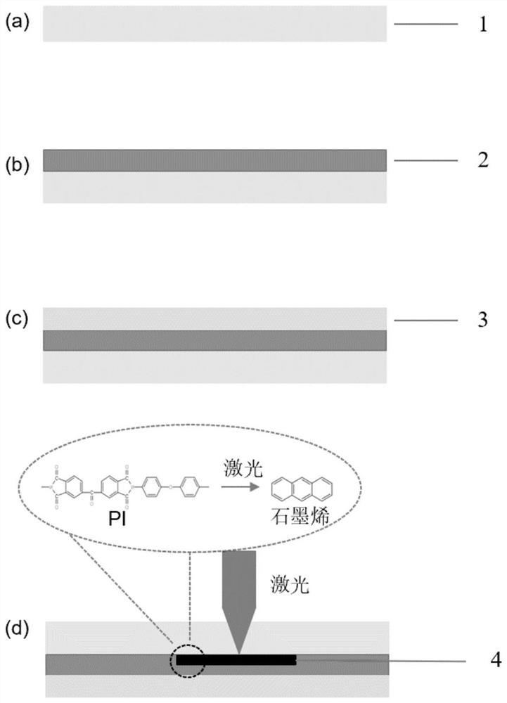
[0038] The preparation method for preparing a composite film of a multilayer interconnected conductive circuit (abbreviated as a composite film of a multilayer interconnected conductive circuit) comprises the following steps:

[0039] First, a light-absorbing polymer layer is prepared on a substrate in the manner described above to obtain a two-layer structure; then, a mask having a single hole is attached to the surface of a two-layer light-absorbing polymer layer, and After depositing a layer of light-absorbing polymer material on the film, the mask is removed to ensure that only the position corresponding to the single hole is deposited with light-absorbing polymer material, and then cured to form a light-absorbing polymer connecting column. Next, prepare an encapsulation layer on the surface of the light-absorbing polymer layer on which the light-absorbing polymer connection posts are formed (the encapsulation layer mainly plays the role of bonding the upper and lower two-l...

Embodiment 1

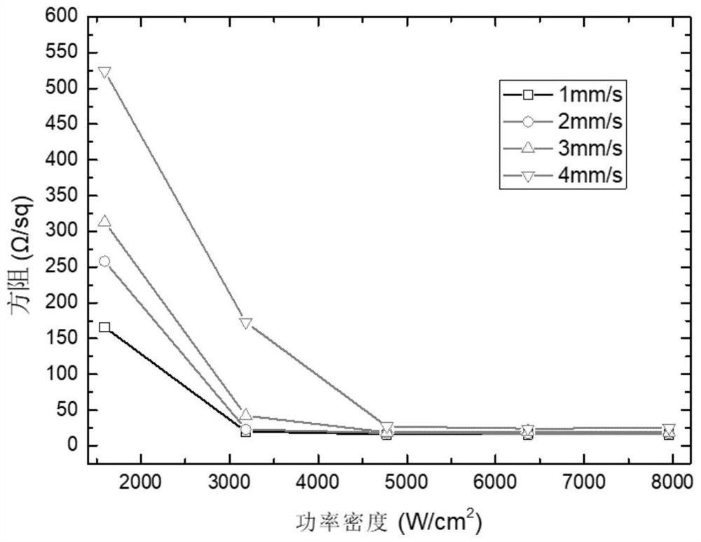
[0050] For a single-layer strain sensor, first spin-coat a layer of PI on the cleaned quartz glass sheet and place two thin wires on the edge, and then continue to use the spin-coating process on the obtained quartz glass / The surface of the PI film is then spin-coated with a layer of epoxy resin film; after that, the obtained film sample is placed on the XY motion platform of the laser test bench, and the height and horizontal position of the XY motion platform are adjusted so that the laser spot is located at the center of the film sample. At the position of one of the thin wires, the two ends of the laser scanning pattern overlap with the two thin wires; then, adjust the energy density and scanning speed of the laser, and the laser irradiates the light-absorbing polymer inside the interlayer through the laser transparent substrate material on the top On the surface, the irradiated polymer will absorb the energy of photons to undergo photothermal or photochemical decompositio...

Embodiment 2

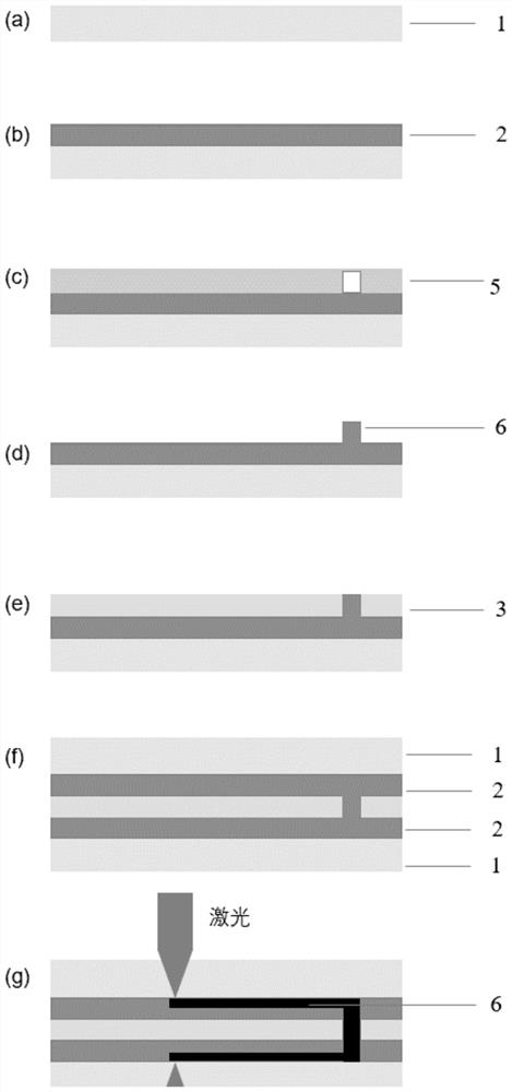
[0059] see figure 2 , the laser processing method of the multilayer structure embedded with multilayer interconnected planar inductors and planar capacitors provided by Embodiment 2 of the present invention mainly includes the following steps:

[0060] (1) Adopting the method in the laser embedded processing single-layer patterned conductive circuit step (1) to clean the quartz glass and the method of spin coating in the step (2) to prepare two samples of quartz glass / PI;

[0061] (2) Paste a mask with a single hole on the PI surface of one of the samples, spin coat a layer of PI on the surface, tear off the mask to ensure that only the single hole contains PI, and then cure to obtain light-absorbing polymerization Connect column 6.

[0062] (3) Prepare epoxy resin by the method in step (3) of laser embedded processing single-layer patterned conductive circuit, then spin-coat a layer of epoxy resin on the surface of quartz glass / PI sample, and prepare in step (1) Another piec...


PUM

PropertyMeasurementUnit
wavelengthaaaaaaaaaa

Abstract

The invention belongs to the related technical field of laser processing and preparation of circuits, and discloses a multi-layer structure with an internal embedded circuit and a non-contact laser processing method thereof. The method comprises the following steps that (1) a composite film is provided and is of a layered structure, and the composite film comprises a substrate, a light absorption polymerization layer formed on the substrate and a packaging layer formed on the light absorption polymerization layer; and (2) the composite film is scanned by using laser, the laser penetrates through the substrate and then irradiates the light absorption polymerization layer, carbonization decomposition is conducted on the region of the light absorption polymerization layer irradiated by the laser, and a patterned conductive circuit is formed by residues obtained by means of carbonization decomposition, and the laser selectively carbonizes the region of the light absorption polymerization layer in the interlayer to form the patterned conductive circuit, so that the embedded circuit is prepared in the multi-layer structure. The method is simple in process and low in cost, and solves the problem of electrode breakage caused by large seal deformation in the traditional transfer printing process and the stress mismatching effect in the packaging process.

Description

technical field [0001] The invention belongs to the technical field related to laser processing and preparation of circuits, and more specifically relates to a multilayer structure with embedded circuits inside and a non-contact laser processing method thereof. Background technique [0002] The formation of conductive circuits on the surface of different materials plays a very important role in both academic research and industrial technology. As early as the 1950s, British scientist G.W.A. Dummer first proposed the idea of ​​integrated circuits, and within a few years Clair Kilby and Robert Noyce made this idea a reality. The core of integrated circuit manufacturing is to use a certain process to interconnect different devices, different materials and different structures on the silicon substrate to realize their corresponding functions. With the continuous advancement of technology, flexible electronics and curved surface electronics have emerged at the historic moment. I...

Claims


Application Information

Patent Timeline
Patent Type & Authority Applications(China)
IPC IPC(8): B23K26/362B23K26/082
CPCB23K26/362B23K26/082
Inventor 黄永安余海洋
Owner HUAZHONG UNIV OF SCI & TECH
Why Eureka
Try Eureka