A kind of high quality ilmenite structure zinc metatitanate single crystal thin film and its preparation method and application
A technology of zinc metatitanate and single crystal thin film, which is applied in the direction of single crystal growth, single crystal growth, chemical instruments and methods, etc., can solve the problem of rarely considering the lattice mismatch between the film and the substrate, and has not yet seen zinc metatitanate Single crystal thin film materials, lack of semiconductor optoelectronic properties and other problems, to achieve the effect of less defects, complete lattice arrangement, and complete lattice structure
- Summary
- Abstract
- Description
- Claims
- Application Information
AI Technical Summary
Problems solved by technology
Method used
Image
Examples
Embodiment 1
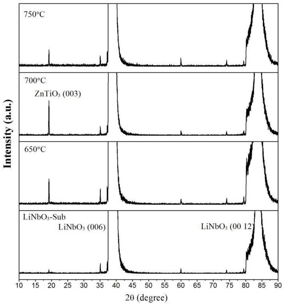
[0062] with LiNbO 3 (006) is the substrate, 99.99% of the ceramic target is used as the target material, and the zinc metatitanate thin film is prepared by the PLD technology.
[0063] Proceed as follows:
[0064] (1) The clean LiNbO 3 (006) The substrate and the zinc metatitanate target are respectively placed at the positions of the substrate and the target in the reaction chamber, and the reaction chamber is closed. Turn on the molecular pump and pump the reaction chamber to a high vacuum, the vacuum degree is 8.5×10 -5 Pa, the substrate base is heated to 700°C;
[0065] (2) Open the high-purity oxygen bottle, feed oxygen into the reaction chamber, control the oxygen flow rate to 20sccm with a gas flow meter, adjust the valve of the reaction chamber, stabilize the pressure of the reaction chamber at 5Pa, and keep it for 30 minutes;
[0066] (3) Turn on the laser, adjust the laser to the energy stable mode, the single pulse energy is 200mJ, the burst length is 20ns, and ...
Embodiment 2
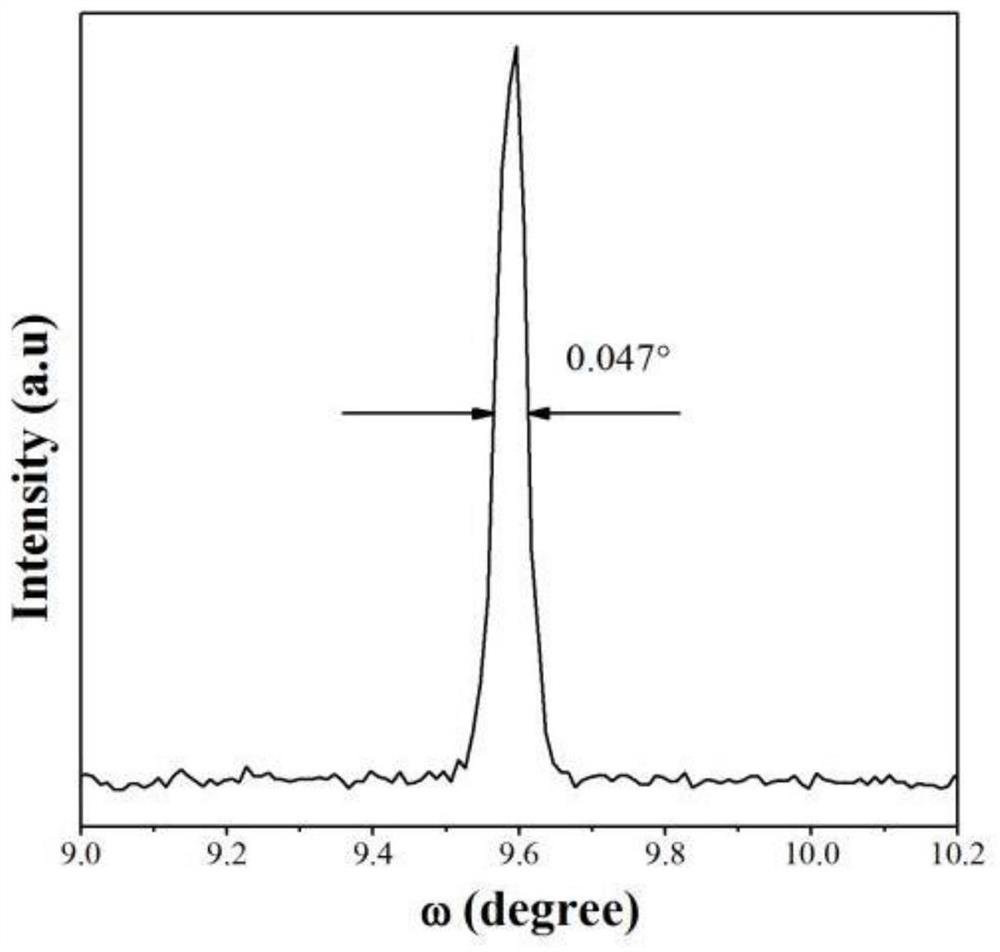
[0074] Preparation of ZnTiO by PLD Technology 3 The single crystal thin film, the used target and substrate and the preparation process are the same as those in Example 1, the difference is that the substrate temperature is 650°C. ZnTiO prepared in this example 3 The film has a single epitaxial orientation of the (003) crystal plane, but compared with Example 1, ZnTiO 3 The diffraction peak intensity of the (003) crystal plane decreased, and the full width at half maximum also increased, indicating that the quality of the thin film single crystal prepared at the substrate temperature decreased.
Embodiment 3
[0076] Preparation of ZnTiO by PLD Technology 3 The single crystal thin film, the used target material and substrate, and the preparation process are the same as those in Example 1, except that the substrate temperature is 750°C. ZnTiO prepared in this example 3 The film has a single epitaxial orientation of the (003) crystal plane. Compared with Example 1, the changes of the diffraction peak intensity and peak width of the (003) crystal plane of the film all indicate that the crystal quality of the film decreases.
PUM
| Property | Measurement | Unit |
|---|---|---|
| diameter | aaaaa | aaaaa |
| optical band gap | aaaaa | aaaaa |
Abstract
Description
Claims
Application Information


