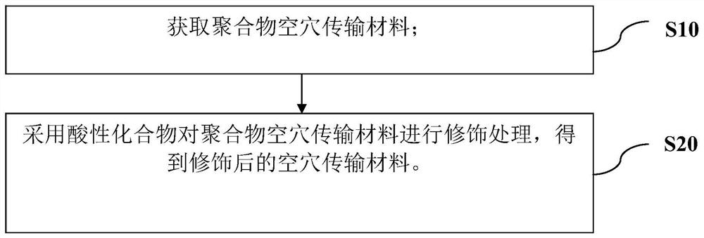
Modification method of hole transport material, light-emitting device and preparation method of light-emitting device
A technology of hole transport material and modification method, which is applied in the field of display devices, can solve the problems of large energy gap between the hole transport layer and the quantum dot light-emitting layer, so as to improve luminous efficiency and stability, reduce energy level difference, and improve recombination efficiency effect
- Summary
- Abstract
- Description
- Claims
- Application Information
AI Technical Summary
Problems solved by technology
Method used
Image
Examples
preparation example Construction
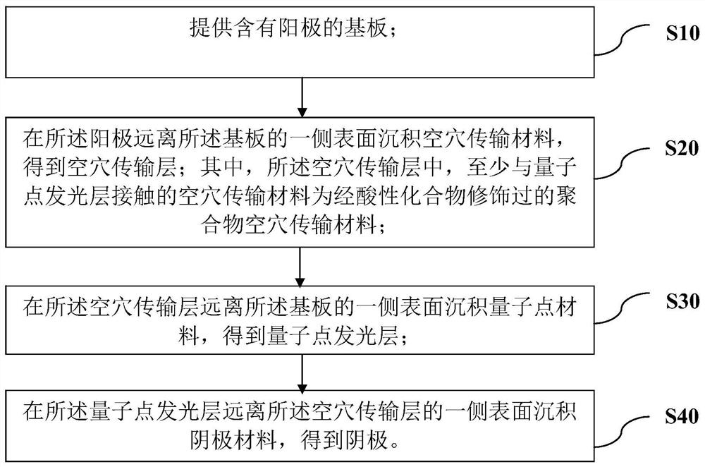
[0041] The second aspect of the present application provides a method for preparing a light-emitting device, comprising the following steps:
[0042] S10. Providing a substrate comprising an anode,
[0043] S20. Depositing a hole transport material on the surface of the anode away from the substrate to obtain a hole transport layer;
[0044] S30. Depositing a quantum dot material on the surface of the hole transport layer away from the substrate to obtain a quantum dot light-emitting layer;
[0045] S40. Depositing a cathode material on the surface of the quantum dot luminescent layer away from the hole transport layer to obtain a cathode;
[0046] Wherein, the side of the hole transport layer close to the quantum dot light-emitting layer contains a polymer hole transport material modified with an acidic compound.
[0047] In the method for preparing a light-emitting device provided in the second aspect of the present application, a hole transport layer, a quantum dot light-...
Embodiment 1
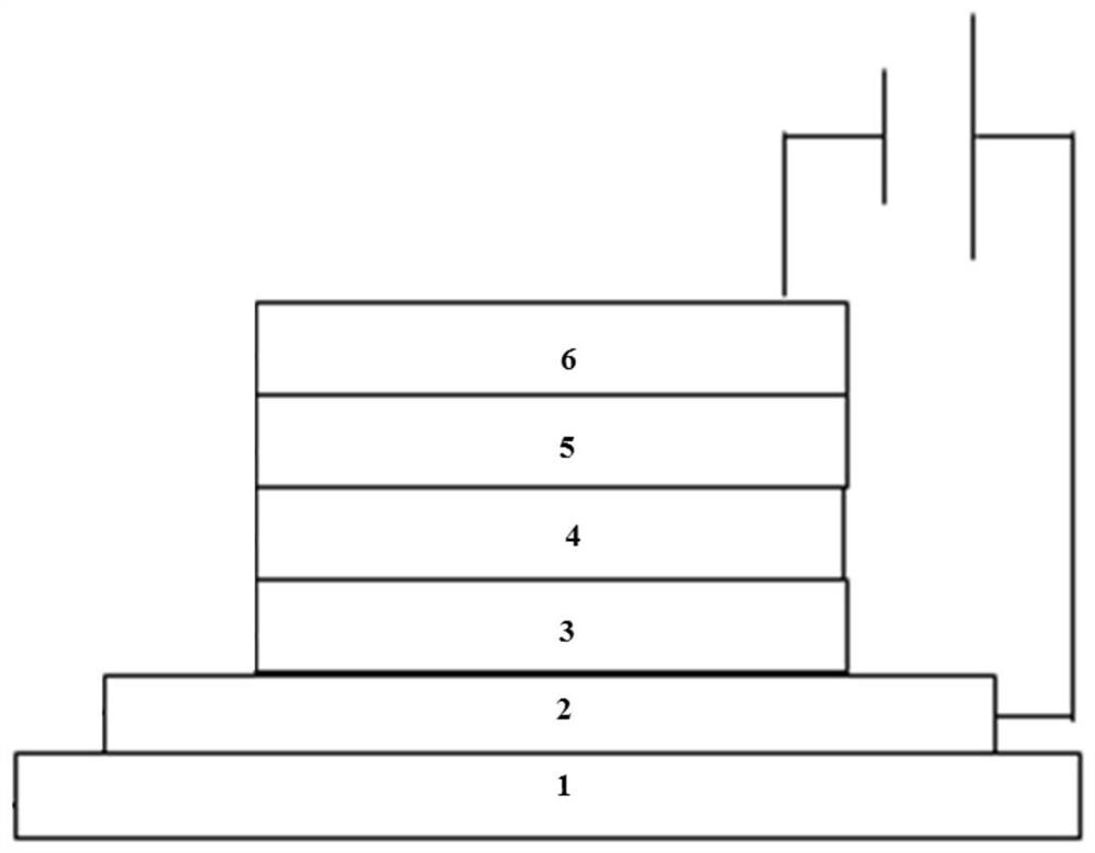
[0082] A quantum dot light emitting diode, comprising the following steps:
[0083] 001 spin-coated PEDOT:PSS on a clean ITO substrate as a hole injection layer. And heated at 150°C for 30min.
[0084] 002 Continue to spin-coat 8 mg / mL TFB solution on the PEDOT:PSS film as a hole transport layer.
[0085] 003 Spin-coat hydrogen bromide ethanol solution on TFB film, its pH value is 5. Anneal at 150°C for 30min after spin coating. The solution used can also be an ethanol solution of organic acids such as phosphoric acid or acetic acid.
[0086] 004 Spin-coat green light quantum dots on the hole transport layer as the light-emitting layer.
[0087] 005 continued to spin-coat zinc oxide on the quantum dot film as an electron transport layer.
[0088] 006 Evaporate a metal Ag electrode on the electron transport layer.
[0089] 007 device packaging to obtain quantum dot light-emitting diodes.
Embodiment 2
[0091] A quantum dot light emitting diode, comprising the following steps:
[0092] 001 spin-coated PEDOT:PSS on a clean ITO substrate as a hole injection layer. And heated at 150°C for 30min.
[0093] 002 Spin-coat the TFB chlorobenzene solution with hydrogen bromide as an additive on the PEDOT:PSS film, and the addition ratio is 8*10 -5 mol HBr per ml TFB chlorobenzene solution. TFB solution is 8mg / mL. The acid used as an additive may also be an organic acid such as phosphoric acid or acetic acid.
[0094] 003 Spin-coat green light quantum dots on the above-mentioned hole transport layer as the light-emitting layer.
[0095] 004 continued to spin-coat zinc oxide on the quantum dot film as an electron transport layer.
[0096] 005 Evaporate a metal Ag electrode on the electron transport layer.
[0097] 006 device packaging to obtain quantum dot light-emitting diodes.
PUM
| Property | Measurement | Unit |
|---|---|---|
| particle diameter | aaaaa | aaaaa |
Abstract
Description
Claims
Application Information
 - R&D
- Intellectual Property
- Life Sciences
- Materials
- Tech Scout
- Unparalleled Data Quality
- Higher Quality Content
- 60% Fewer Hallucinations
Browse by: Latest US Patents, China's latest patents, Technical Efficacy Thesaurus, Application Domain, Technology Topic, Popular Technical Reports.
© 2025 PatSnap. All rights reserved.Legal|Privacy policy|Modern Slavery Act Transparency Statement|Sitemap|About US| Contact US: help@patsnap.com


