
Neuron structure based on partial depletion type silicon-on-insulator and working method thereof

A silicon-on-insulator, depletion-type technology, applied in the field of neuron structure, can solve the problems of CMOS synapse incompatibility, large unit area occupation, complex manufacturing process, etc., to achieve increased integration density, reduced occupied area, and simple manufacturing process Effect

Pending Publication Date: 2022-02-15
天津市滨海新区微电子研究院
View PDF0 Cites 0 Cited by
  • Summary
  • Abstract
  • Description
  • Claims
  • Application Information

AI Technical Summary

Problems solved by technology

[0005] In view of this, the present invention provides a neuron structure based on partially depleted silicon-on-insulator to solve the problems in the prior art that the unit area of ​​the neuron device is large, the structure is not simple enough, the manufacturing process is complicated, and the CMOS synapse is not compatible. The problem

Method used


Image

  • Neuron structure based on partial depletion type silicon-on-insulator and working method thereof
  • Neuron structure based on partial depletion type silicon-on-insulator and working method thereof

Examples


Embodiment 1

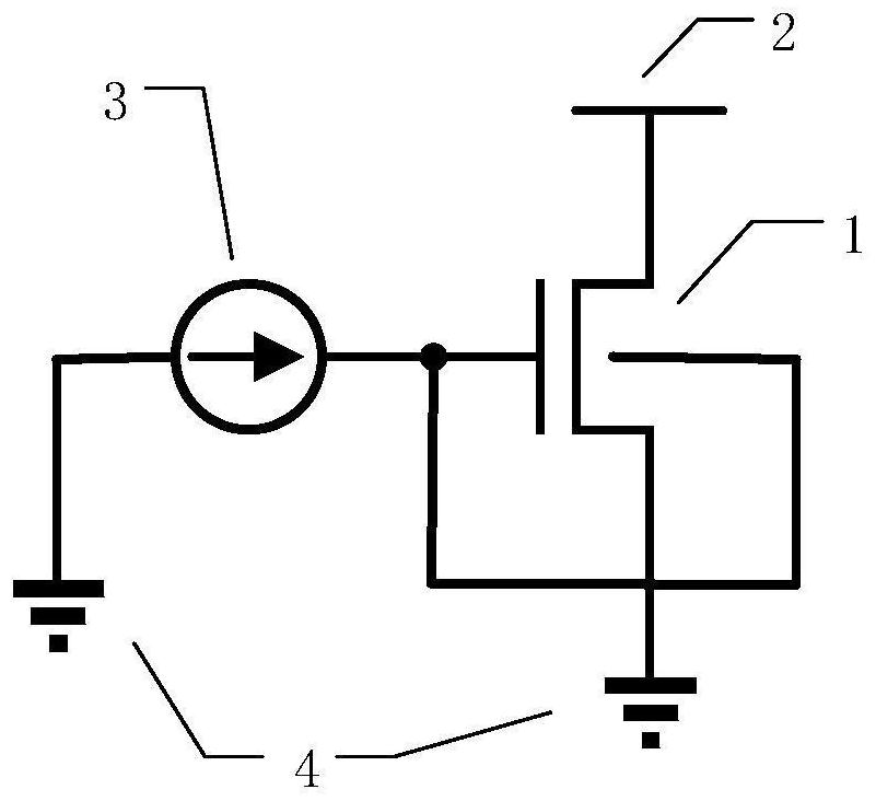
[0042]In this embodiment, the gate length of the NMOS PD-SOI transistor 1 is 5nm-1um, so as to ensure that the leakage caused by the input current will not affect the spike characteristics of the LIF neurons. Longer gate lengths result in higher peak voltages and improved noise margins, but at the same time lead to higher power dissipation.

Embodiment 2

[0044] In this embodiment, the NMOS PD-SOI transistor 1 is fabricated on an SOI wafer with a buried oxide layer thickness of 10nm-1um. The thickness of the buried oxide layer must ensure that the device is isolated from the outside world, so that the current source can operate on a single device without affect other devices.

Embodiment 3

[0046] In this embodiment, the output current of the constant current source 3 is 10pA to 100nA. Since the transistor structure itself has a certain leakage, the normal charging step may not be realized if it is lower than 10pA, and the transistor may be damaged if it is higher than 100nA. The breakdown of the pn junction in the cell prevents normal neuron characteristics from being displayed. At the same time, the size of the current source will affect the frequency characteristics of the spike.


PUM


Abstract

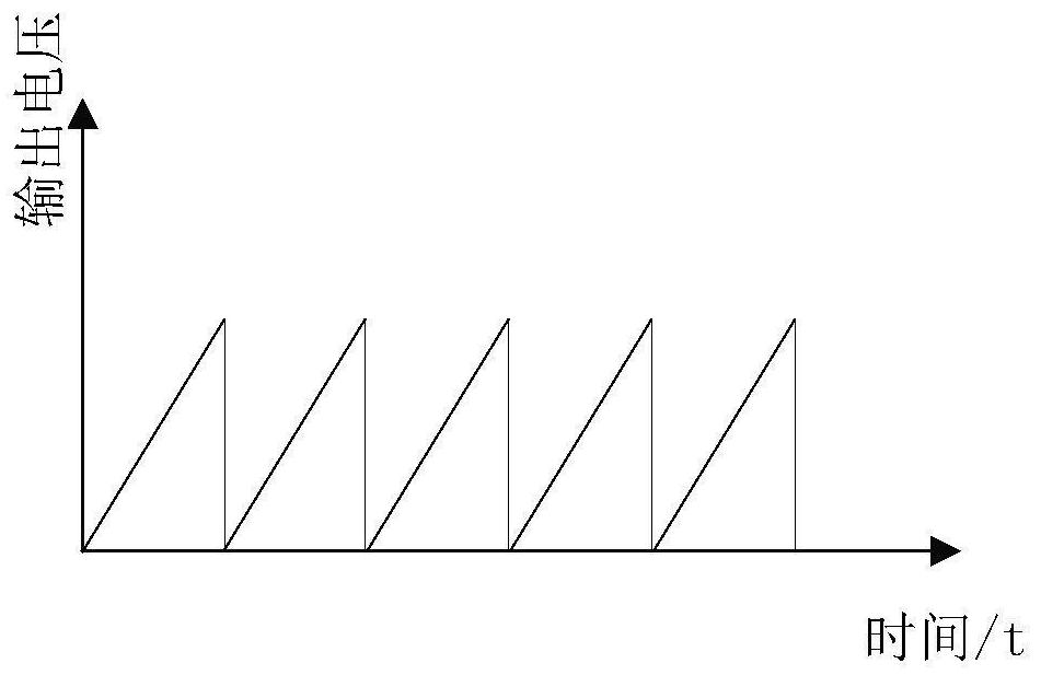
The invention provides a neuron structure based on partial depletion type silicon-on-insulator and a working method thereof. The structure comprises a PD-SOI NMOS transistor, the drain electrode of the PD-SOI NMOS transistor receiving a constant voltage, and the grid electrode and the body electrode of the PD-SOI NMOS transistor receiving a constant current; and the source electrode is grounded. According to the invention, an LIF neuron model is used, a single NMOS PD-SOI transistor is adopted, the body potential of the PD-SOI device can be effectively controlled because the body and the substrate of the PD-SOI device are isolated by an oxide layer, and each neuron can be isolated by the oxide layer, so that a single neuron can be conveniently operated by using current; a single PD-SOI transistor is used for realizing the function of an LIF neuron, and an SOI floating body effect is used for accumulating and transmitting charges so as to replace a capacitor and a reset circuit; compared with a neuron based on a CMOS complex circuit structure, a large number of circuit structures such as transistors and capacitors are omitted, the occupied area of the unit structure is reduced, and the integration density can be improved if a neural network is constructed.

Description

technical field [0001] The invention relates to the technical field of semiconductor devices, in particular to a neuron structure based on partially depleted silicon-on-insulator. Background technique [0002] In the artificial neural network hardware structure, the neuron device is one of its basic unit components, and its performance and structure determine the performance and integration density of the neuron network. Among various neuron models, the leaky set firing (LIF—leaky-integrate and fire) neuron model has relatively high accuracy and simplicity. Therefore, it is most feasible to use the LIF neuron model as the hardware structure to realize the artificial neural network. [0003] The LIF model is a neuron model that imitates a biological neuron that receives input current from a synapse and triggers an output action voltage when the membrane potential reaches a threshold. In this model, charge accumulates in the capacitor, and when the threshold voltage is reach...

Claims


Application Information

Patent Timeline
Patent Type & Authority Applications(China)
IPC IPC(8): H01L27/12H01L29/78
CPCH01L27/1203H01L27/1207H01L29/78
Inventor 毕津顺
Owner 天津市滨海新区微电子研究院
Learn More