N-type Bi-Te-Se-based thermoelectric thin film and preparation method thereof
A bi-te-se, thermoelectric thin film technology, applied in the manufacture/processing of thermoelectric devices, junction lead-out materials of thermoelectric devices, vacuum evaporation coating, etc. Loss and other problems, to achieve the effect of good thermoelectric performance, good quality and good repeatability
- Summary
- Abstract
- Description
- Claims
- Application Information
AI Technical Summary
Problems solved by technology
Method used
Image
Examples
Embodiment 1
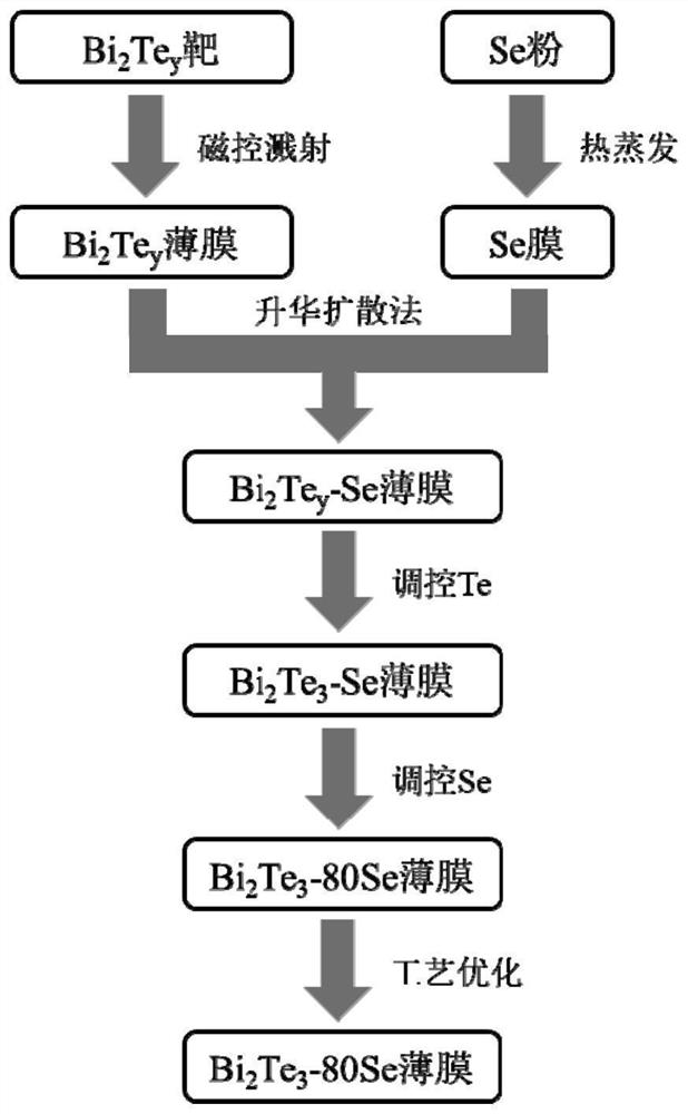
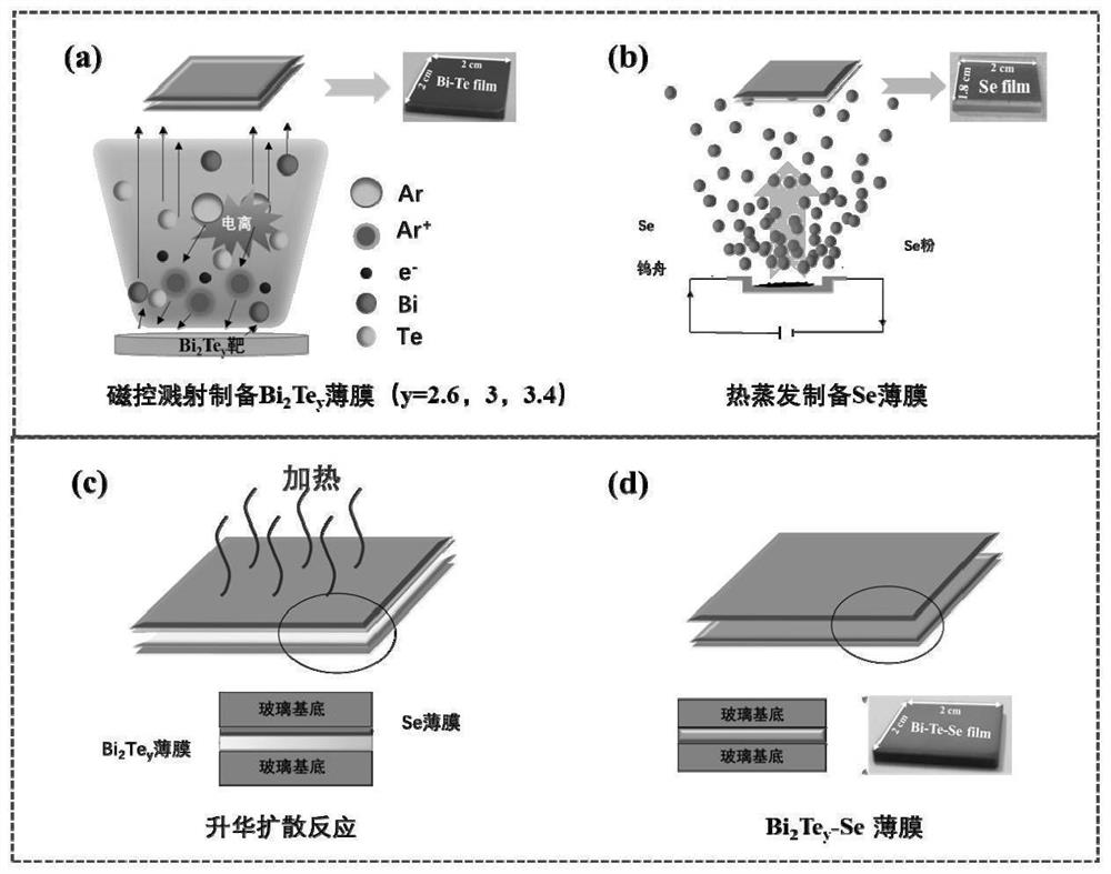
[0055] Based on 2cm×2cm glass, with Bi 2 Te 3 The target material is magnetron sputtering, and the magnetron sputtering parameters are set as follows: the power is 30W, and a Bi with a thickness of 900nm is prepared on the glass substrate. 2 Te 3 film.
[0056] Using 2cm×2cm glass as the substrate and Se powder as the Se source for thermal evaporation, the parameters of thermal evaporation are set as follows: the evaporation current is 20A, the mass of Se powder is 0.05g, and a Se film with a thickness of 40nm is prepared on the glass substrate .
[0057] Bi on the glass substrate 2 Te 3 The thin film and the Se thin film on the glass substrate are set face to face (the inner side is Bi 2 Te 3 Thin film and Se thin film, two glass substrates on the outside, specifically as figure 2 shown in (c)), and seal the gap between the two outer glass substrates with a sealant, wrap it with aluminum foil, and heat treat it at a temperature of 300°C for 40min to obtain an N-type ...
Embodiment 2
[0059] Bi 2 Te 3 The preparation of the film is the same as in Example 1.
[0060] Using 2cm×2cm glass as the substrate and Se powder as the Se source for thermal evaporation, the parameters of thermal evaporation are set as follows: the evaporation current is 20A, the mass of Se powder is 0.1g, and a Se film with a thickness of 80nm is prepared on the glass substrate .
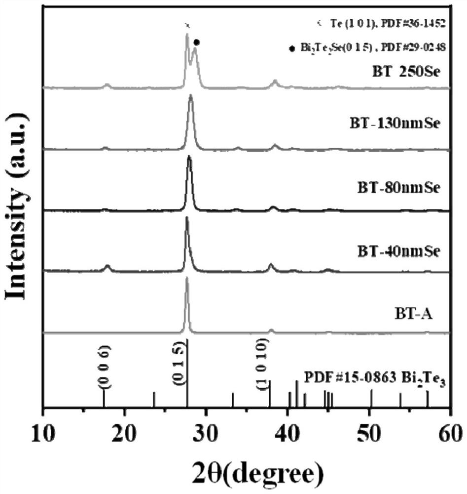
[0061] Bi on the glass substrate 2 Te 3 The thin film and the Se thin film on the glass substrate are set face to face (the inner side is Bi 2 Te 3 Thin film and Se thin film, two glass substrates on the outside, specifically as figure 2 shown in (c)), and seal the gap between the two outer glass substrates with a sealant, wrap it with aluminum foil, and heat treat it at a temperature of 325°C for 40min to obtain an N-type Bi-Te-Se-based thermoelectric film. Denoted as BT-80Se.
Embodiment 3
[0063] Bi 2 Te 3 The preparation of the film is the same as in Example 1.
[0064] The 2cm×2cm glass is used as the substrate, and Se powder is used as the Se source for thermal evaporation. The parameters of the thermal evaporation current are set as follows: the evaporation current is 20A, the mass of Se powder is 0.15g, and Se powder with a thickness of 130nm is prepared on the glass substrate. film.
[0065] Bi on the glass substrate 2 Te 3 The thin film and the Se thin film on the glass substrate are set face to face (the inner side is Bi 2 Te 3 Thin film and Se thin film, two glass substrates on the outside, such as figure 2 shown in (c)), and seal the gap between the two outer glass substrates with a sealant, wrap it with aluminum foil, and heat treat it at a temperature of 325°C for 40min to obtain an N-type Bi-Te-Se-based thermoelectric film. Denoted as BT-130Se.
PUM
| Property | Measurement | Unit |
|---|---|---|
| thickness | aaaaa | aaaaa |
| thickness | aaaaa | aaaaa |
| thickness | aaaaa | aaaaa |
Abstract
Description
Claims
Application Information


