Mirror bit SONOS flash memory unit
A flash memory cell and mirror technology, applied in electrical components, electrical solid-state devices, circuits, etc., can solve problems such as difficulties, and achieve the effects of reducing process costs, saving lithography processes, and improving chip integration.
- Summary
- Abstract
- Description
- Claims
- Application Information
AI Technical Summary
Problems solved by technology
Method used
Image

Examples
Embodiment Construction
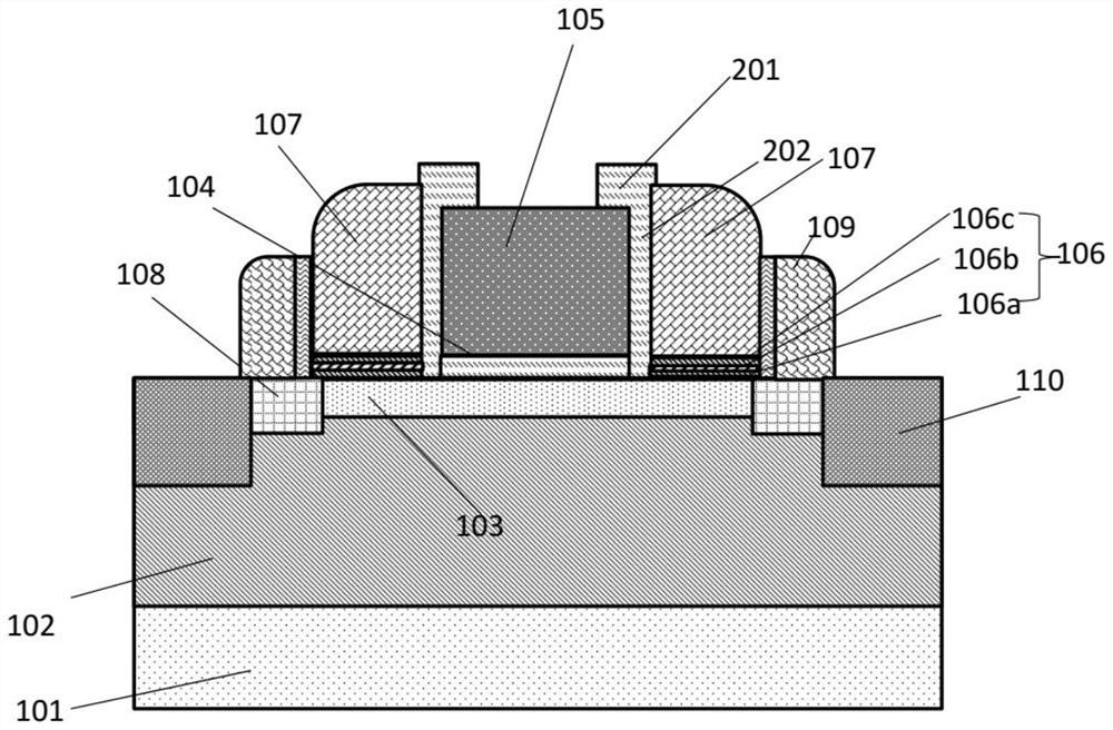
[0040] like figure 1 shown is a schematic structural diagram of a mirror-bit SONOS flash memory cell according to an embodiment of the present invention; the mirror-bit SONOS flash memory cell according to the embodiment of the present invention includes a selection transistor and a storage transistor, and the selection transistor is an enhancement-mode MOS transistor and has a first threshold voltage, The storage transistor is a depletion-mode SONOS storage transistor and has a second threshold voltage in a state where no charge is stored.
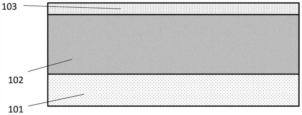
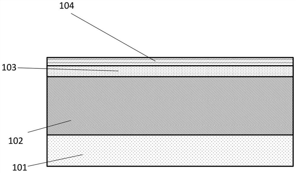
[0041] The selection transistor and the storage transistor share a heavily doped source region and a drain region of the first conductivity type formed on the semiconductor substrate 101, and a surface of the semiconductor substrate 101 between the source region and the drain region is formed with a first conductivity type. A lightly doped channel doping layer 103 of conductivity type. In the embodiment of the present invention, the sour...
PUM
 Abstract
Description
Claims
Application Information
 - R&D
- Intellectual Property
- Life Sciences
- Materials
- Tech Scout
- Unparalleled Data Quality
- Higher Quality Content
- 60% Fewer Hallucinations
Browse by: Latest US Patents, China's latest patents, Technical Efficacy Thesaurus, Application Domain, Technology Topic, Popular Technical Reports.
© 2025 PatSnap. All rights reserved.Legal|Privacy policy|Modern Slavery Act Transparency Statement|Sitemap|About US| Contact US: help@patsnap.com