
FeFET based on anti-ferroelectric gate dielectric and oxide semiconductor channel and preparation method thereof

An oxide semiconductor and antiferroelectric technology, applied in the field of micro-nano electronics, can solve the problems of large operating voltage, breakdown, and insufficient, and achieve the goal of reducing operating voltage, improving durability, reducing charge injection and defect generation Effect

Pending Publication Date: 2022-03-04
PEKING UNIV
View PDF0 Cites 1 Cited by
  • Summary
  • Abstract
  • Description
  • Claims
  • Application Information

AI Technical Summary

Problems solved by technology

At present, hafnium oxide-based FeFETs are mainly facing challenges in durability, which is due to two reasons: in terms of ferroelectric materials, the coercive electric field of hafnium oxide-based ferroelectric materials is relatively large, which makes the operating voltage of the device relatively large, while large voltage It will introduce more charge injection and easily generate new defects; in terms of device structure, the usually existing ferroelectric-semiconductor interface intermediate layer bears a high electric field, which is easy to cause breakdown, and the tunneling current leads to new defects. Gradually close the memory window during the loop
The durability of FeFET at this stage is usually in the 10 5 This is far from enough for the application requirements of non-volatile storage

Method used


Image

  • FeFET based on anti-ferroelectric gate dielectric and oxide semiconductor channel and preparation method thereof
  • FeFET based on anti-ferroelectric gate dielectric and oxide semiconductor channel and preparation method thereof
  • FeFET based on anti-ferroelectric gate dielectric and oxide semiconductor channel and preparation method thereof

Examples


Embodiment Construction

[0044] The present invention will be further described through the embodiments below in conjunction with the accompanying drawings.

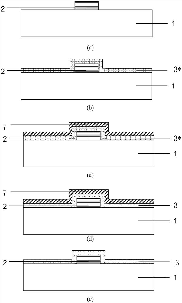
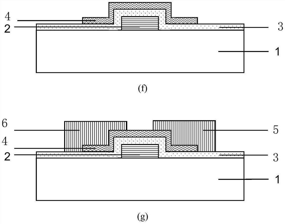
[0045] Such as figure 1 As shown, the high-durability FeFET based on the antiferroelectric gate dielectric and the oxide semiconductor channel of the present invention includes an insulating substrate 1, a back gate electrode layer 2, an activated antiferroelectric gate dielectric material layer 3, and an oxide semiconductor channel 4. The source electrode 5 and the drain electrode 6 . Wherein, the patterned gate electrode layer 2 is located on the insulating substrate 1, the activated antiferroelectric gate dielectric material layer 3 is located on the insulating substrate 1 and the gate electrode layer 2, and the patterned oxide semiconductor channel 4 is located on the activated Above the final antiferroelectric gate dielectric material layer 3 , the source contact electrode 5 and the drain contact electrode 6 are respectively located on the...


PUM

PropertyMeasurementUnit
thicknessaaaaaaaaaa
thicknessaaaaaaaaaa
thicknessaaaaaaaaaa

Abstract

The invention provides a FeFET based on an anti-ferroelectric gate medium and an oxide semiconductor channel and a preparation method of the FeFET, and belongs to the field of micro-nano electronics. The FeFET device comprises an insulating substrate, a patterned back gate electrode layer is arranged on the insulating substrate, an anti-ferroelectric gate dielectric material layer is arranged on the back gate electrode layer, an oxide semiconductor material layer is arranged on the anti-ferroelectric gate dielectric layer and serves as a channel, and a source contact electrode and a drain contact electrode are arranged on the left side and the right side of the upper portion of the channel respectively. The work function difference between the back gate electrode layer and the oxide semiconductor material layer is 1 eV to 2 eV, a built-in electric field is provided for the anti-ferroelectric gate dielectric material layer, and the anti-ferroelectric gate dielectric material forms two different storage states. The anti-ferroelectric gate dielectric is used for replacing a traditional ferroelectric gate dielectric, and the oxide semiconductor channel is used for replacing a traditional silicon-based channel, so that the durability of the memory device is improved.

Description

technical field [0001] The invention belongs to the technical field of micro-nano electronics, and in particular relates to a high-durability FeFET based on an antiferroelectric gate dielectric and an oxide semiconductor channel and a preparation method thereof. Background technique [0002] With the continuous development of integrated circuits, logic and storage devices continue to develop as two basic routes. The size of devices continues to decrease, and the degree of integration continues to increase, from planar integration to three-dimensional integration. In the traditional von Neumann architecture system, computing and storage are separated, and there is a bottleneck of the storage wall. Data transmission not only consumes a lot of power consumption, but also severely limits the development of computing power. In order to break the memory wall and meet the needs of storage-computing fusion trend, a series of new memories with high speed, high density, and low power ...

Claims


Application Information

Patent Timeline
Patent Type & Authority Applications(China)
IPC IPC(8): H01L29/786H01L29/51H01L21/34
CPCH01L29/66969H01L29/78696H01L29/7869H01L29/516
Inventor 唐克超梁中新黄如
Owner PEKING UNIV
Learn More