Mode-insensitive optical waveguide type optical switch and preparation method thereof

An optical waveguide and optical switch technology, applied in the directions of optical waveguides, light guides, optics, etc., can solve the problems of limiting the application of mode division multiplexing systems, mode sensitivity, etc., and achieve mode insensitivity, high preparation efficiency, and low production cost. Effect

Pending Publication Date: 2022-03-08
JILIN UNIV
View PDF2 Cites 1 Cited by
  • Summary
  • Abstract
  • Description
  • Claims
  • Application Information

AI Technical Summary

Problems solved by technology

However, the traditional MZI waveguide optical switch is sensitive to the mode and can only realize the

Method used


Image

  • Mode-insensitive optical waveguide type optical switch and preparation method thereof
  • Mode-insensitive optical waveguide type optical switch and preparation method thereof
  • Mode-insensitive optical waveguide type optical switch and preparation method thereof

Examples


Embodiment 1

[0064] The present invention will be further described below in conjunction with the accompanying drawings and embodiments.

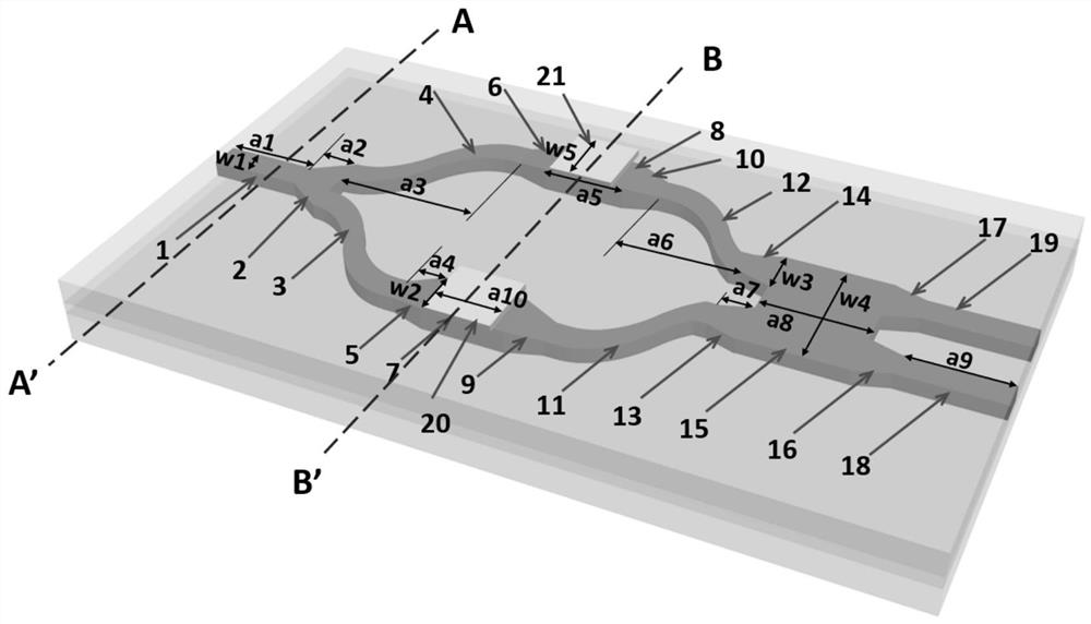
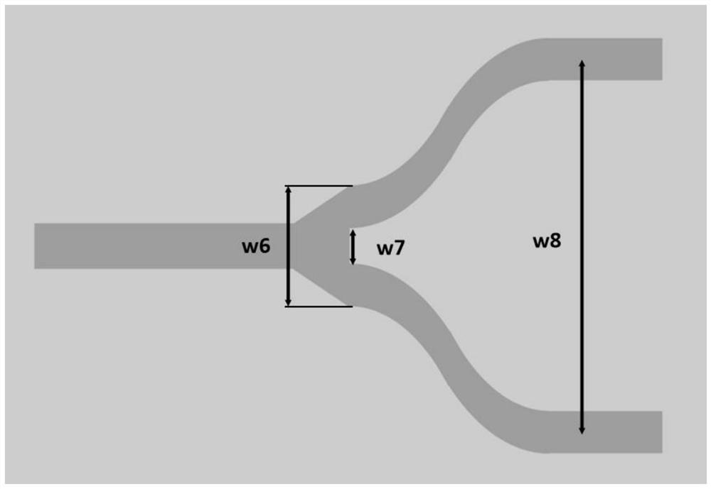
[0065] Example structure such as figure 1 As shown, the input straight waveguide 1, the lengths a1 and a9 of the first output straight waveguide 18 and the second output straight waveguide 19 are equal to 1000 μm; the length a2 of the input tapered waveguide 2 is 635 μm; the first curved waveguide 3, the second curved waveguide The length a3 of the waveguide 4 is equal to 1950 μm; the length a4 of the first connection tapered waveguide 5, the second connection tapered waveguide 6, the third connection tapered waveguide 9, and the fourth connection tapered waveguide 10 is 2100 μm; modulation The length a5 of the arm 7 and the modulation arm 8 is equal to 2000 μm; the length a6 of the third curved waveguide 11 and the fourth curved waveguide 12 is equal to 1950 μm; the first MMI enters the tapered waveguide 13, the second MMI enters the tapered waveguide ...

Embodiment 2

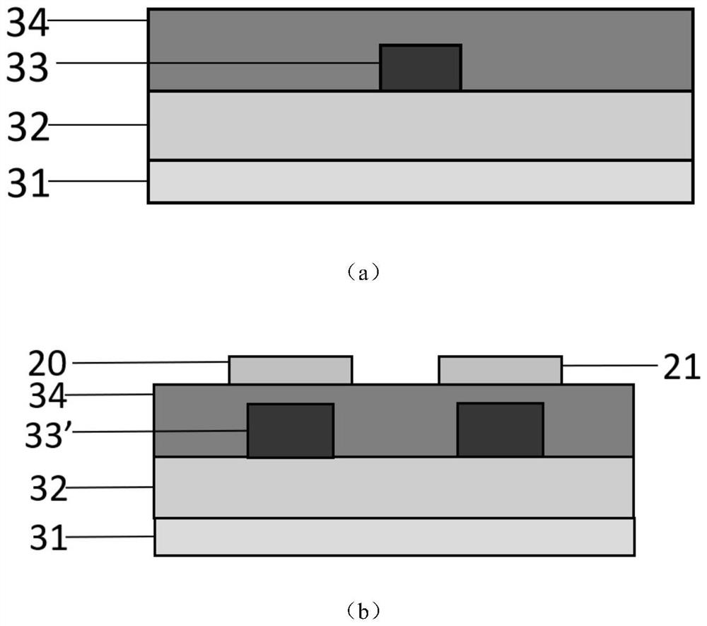
[0078] Cleaning of the silicon wafer substrate 31: Wipe the silicon wafer substrate 31 repeatedly in sequence with acetone and ethanol cotton balls, then rinse it with deionized water, and then dry it with nitrogen, then place the cleaned silicon wafer at a temperature of 120°C Bake for 1 hour to remove moisture;

[0079] Preparation of the polymer lower cladding layer 32: spin-coat the organic polymer lower cladding material EpoClad on the cleaned silicon wafer substrate 31 by using a spin-coating process at a speed of 1800 rpm, and then bake at 120°C Bake for 5 minutes, expose the whole body for 20s, and then bake for 3 minutes at 120°C to obtain a polymer lower cladding layer with a thickness of 7μm

[0080] C: Preparation of polymer core layers 33 and 33'

[0081] The organic polymer core material EpoCore was spin-coated on the prepared lower cladding layer by spin-coating process at a speed of 1500 rpm, then baked at 85°C for 10 minutes, and naturally cooled to room temp...


PUM

PropertyMeasurementUnit
Lengthaaaaaaaaaa
Thicknessaaaaaaaaaa
Thicknessaaaaaaaaaa

Abstract

The invention discloses a mode-insensitive optical waveguide type optical switch and a preparation method thereof, and belongs to the technical field of planar optical waveguide optical switches and preparation. The mode-insensitive optical waveguide type optical switch is prepared by taking a silicon wafer as a substrate, taking an organic polymer material as a lower cladding and an upper cladding of a waveguide and taking an organic polymer material with a relatively large thermo-optical coefficient as a core layer of the waveguide. The advantages of various types, high processability and large thermo-optical coefficient of organic polymer materials are fully utilized, the refractive index of the modulation arm is changed by changing the temperature of the modulation arm, then the phase of light in the modulation arm is changed, and the purpose of changing an output port of light is achieved; the thickness of the modulation arm is adjusted through reactive ion etching, so that the effective refractive indexes of different modes are almost the same, the modulation temperatures required by different optical modes are the same, and the purpose that the modes are insensitive is achieved. The planar optical waveguide optical switch is low in cost, high in preparation efficiency and suitable for batch production and practical application.

Description

technical field [0001] The invention belongs to the field of planar optical waveguide optical switch and its preparation technology, and specifically relates to a lower cladding layer, an upper cladding layer, and a core layer of an optical waveguide structure with silicon wafers as the substrate and organic polymer materials with different refractive indices as the optical waveguide structure respectively. A mode-insensitive optical waveguide-type optical switch and a method for preparing the same. Background technique [0002] With the rapid development of science and technology, the way of sending and obtaining information is more convenient and faster. However, the huge amount of communication data poses a great challenge to the transmission capacity of the information transmission system. How to improve data transmission speed and transmission capacity has become an important problem to be solved urgently, and the emergence of optical communication has become the key t...

Claims


Application Information

Patent Timeline
IPC IPC(8): G02B6/12G02B6/122G02B6/125
CPCG02B6/12G02B6/125G02B6/1228G02B6/1221G02B2006/12038G02B2006/12176G02B2006/12145G02B2006/12069
Inventor 王希斌孙士杰林柏竹朱穆廉天航车远华孙雪晴张大明
Owner JILIN UNIV
Why Eureka
Try Eureka