
Eureka
For R&D, Eureka makes reading and utilizing patents & technical documents easy.
Eureka AIR
Designed for self-driven R&D workflows. Generate viable solutions, solve complex R&D challenges, empower your innovation with AI.

Eureka Materials
Designed for material experts only. Revolutionize your material R&D, from search, analyze, to developing new materials.

TechResearch
Generate reliable direction feasibility study reports for your R&D in just a few steps.

TechSeek
Discover and master advanced knowledge NOW. Basics, ideas, possibilities, all at once.

TechMind
As an expert in R&D Theories, TechMind can generates customized viable solutions instantly.

TechRisk
Analyze your overall solution with one click, know your potential R&D risks in advance.

TechMonitor
Get weekly tech updates, stay abreast of the latest tech innovations and key insights.
Solar cell and preparation method thereof
A solar cell and electrode technology, applied in the field of solar cells, can solve the problems of extra, complicated operation, difficult production cost, etc., and achieve the effect of improving the pulling force and the bonding force
- Summary
- Abstract
- Description
- Claims
- Application Information
AI Technical Summary
Problems solved by technology
Method used
Image

Examples
preparation example Construction
[0132] In this application, the first method for preparing a solar cell includes the following steps:
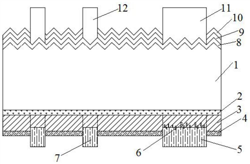
[0133] Step 1: providing a silicon substrate 1 .
[0134] Step 2: Form a doped layer 8 on one side surface (front side or front surface) of the silicon substrate.
[0135] Step 3: setting a tunneling layer 2 on one side surface (back surface or rear surface) of the silicon substrate 1 .
[0136] Step 4: depositing a first doped polysilicon layer 3 on the side of the tunneling layer 2 away from the silicon substrate 1 .
[0137] Step 5: depositing a first dielectric layer 4 on the side of the first doped polysilicon layer 3 away from the tunneling layer 2 .
[0138] Step 6: Printing a first printed electrode paste on the side of the first dielectric layer 4 away from the first doped polysilicon layer 3 to form a first printed sintered layer, and the first printed electrode paste burns through the The first dielectric layer 4 is connected to the first doped polysilicon laye...
Embodiment 1
[0313] The solar cell in this embodiment is the first solar cell, comprising the following steps:
[0314] Step 1: providing a silicon substrate.
[0315] It is obtained by cleaning the silicon wafer, alkali texturing and edge etching. After texturing, a pyramid texture is formed on the front surface (front surface) of the silicon wafer to obtain a p-type crystalline silicon layer.
[0316] Step 2: Form a doped layer
[0317] Boron diffusion on the front side of the silicon substrate forms a doped layer;
[0318] The boron diffusion may be: using a boron source to diffuse the silicon substrate under high temperature conditions, and form a doped layer on the front side through the boron diffusion.
[0319] The boron source for the boron diffusion may include boron tribromide, the diffusion temperature of the boron diffusion ranges from 950-1000°C, and the diffusion time ranges from 1.5-2.5 hours.
[0320] Step 3: forming a tunneling layer.
[0321] In step 2, boron diffusion ...
Embodiment 2
[0354] The solar cell in this embodiment is the second type of solar cell, comprising the following steps:
[0355] Step 1: Provide a silicon substrate (refer to Example 1 for the specific process)
[0356] Step 2: Form the second dielectric layer
[0357] Oxidizing the front side of the silicon substrate to form a silicon oxide layer on the front side of the silicon substrate, that is, the silicon oxide layer is the second dielectric layer.
[0358] Step 3: Forming a tunneling layer (for the specific process, please refer to Example 1)
[0359] Step 4: Forming the first doped polysilicon layer (refer to Example 1 for the specific process)
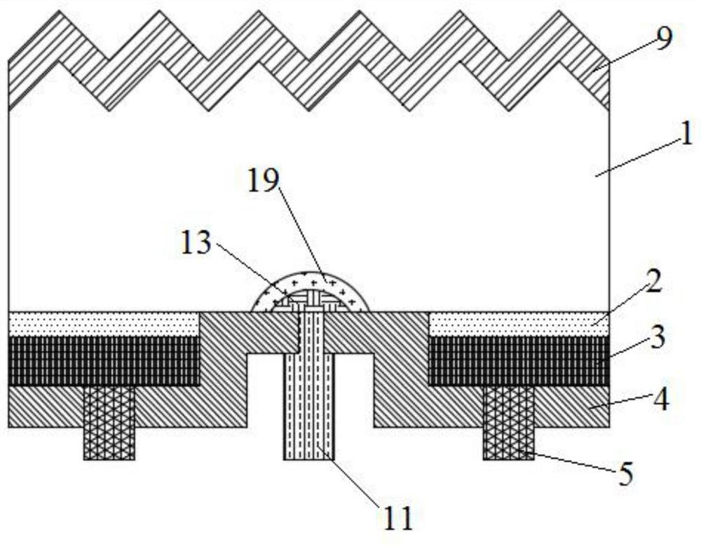
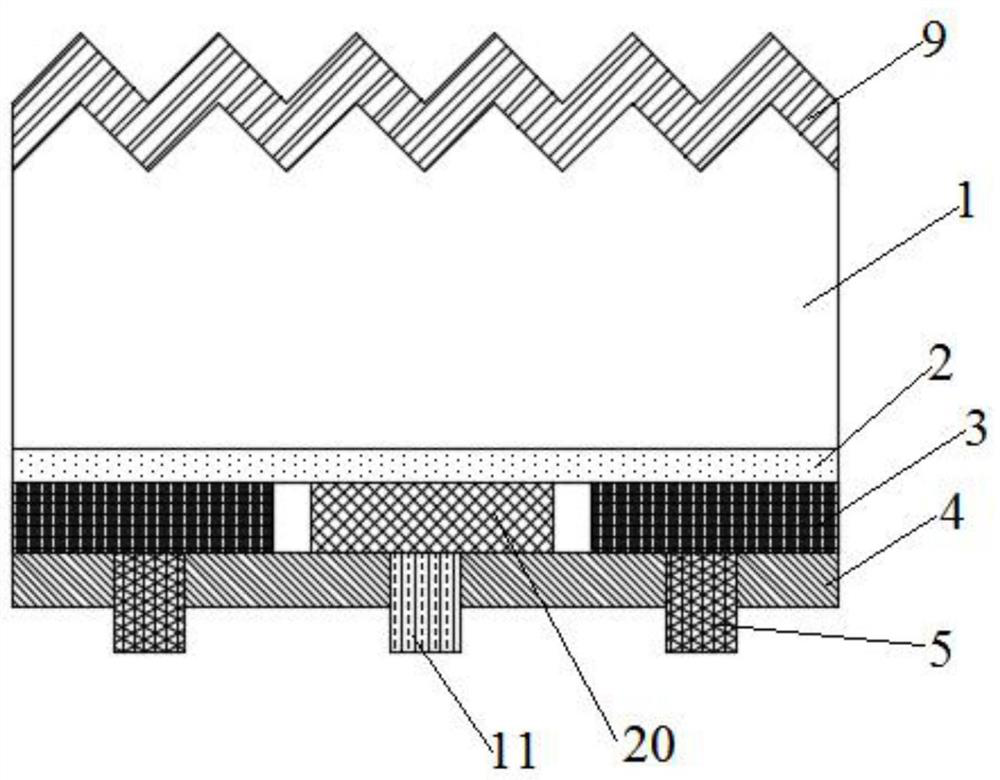
[0360] Step 5: Form the first dielectric layer
[0361] On the surface of the first doped polysilicon layer, a laser is used to ablate the first doped polysilicon layer and the tunneling layer at intervals to expose the silicon base, thereby forming a plurality of interval first regions.
[0362] Deposit a first dielectric layer on the...
PUM
| Property | Measurement | Unit |
|---|---|---|
| thickness | aaaaa | aaaaa |
| thickness | aaaaa | aaaaa |
| refractive index | aaaaa | aaaaa |
Abstract
Description
Claims
Application Information
 - R&D Engineer
- R&D Manager
- IP Professional
- Industry Leading Data Capabilities
- Powerful AI technology
- Patent DNA Extraction
Browse by: Latest US Patents, China's latest patents, Technical Efficacy Thesaurus, Application Domain, Technology Topic, Popular Technical Reports.
© 2024 PatSnap. All rights reserved.Legal|Privacy policy|Modern Slavery Act Transparency Statement|Sitemap|About US| Contact US: help@patsnap.com