
Synthesis and application of high-order superlattice

A superlattice, high-level technology, applied in the field of nanomaterials, can solve the problems of atomic thin crystal degradation, unrealized, limited stability, etc., to achieve the effects of improved performance, excellent structural advantages, and simple and easy operation.

Active Publication Date: 2022-03-18
HUNAN UNIV
View PDF3 Cites 1 Cited by
  • Summary
  • Abstract
  • Description
  • Claims
  • Application Information

AI Technical Summary

Problems solved by technology

This approach is generally suitable for generating a wide variety of heterostructures from a wide variety of layered crystals, but typically has limited yield and reproducibility, and is not useful for generating higher-order superlattices that require an increasing number of stacking steps. language, with exponential difficulty 16-17
Alternatively, chemical vapor deposition (CVD) methods have also been explored for the direct synthesis of 2D vdWH, but are also generally limited to low-order structures with only two distinct blocks.
To produce high-order vdWSLs using the vdWHs epitaxial growth method requires trial and error between different chemical or thermal environments, which often results in severe degradation of atomically thin crystals
Although this challenge can be partially mitigated by the partial success of 2D lateral superlattices through careful synthetic design, higher-order 2D vertical superlattices using similar strategies are more challenging and have not been achieved so far. 18-19
Furthermore, a unique electrochemical molecular intercalation method was recently reported for the creation of high-order superlattices, but only for molecular systems with limited stability
To date, despite enormous efforts and the successful construction of a variety of van der Waals heterojunctions, the construction of high-order stable van der Waals superlattices remains an ongoing challenge

Method used


Image

  • Synthesis and application of high-order superlattice
  • Synthesis and application of high-order superlattice
  • Synthesis and application of high-order superlattice

Examples


Embodiment 1

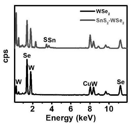
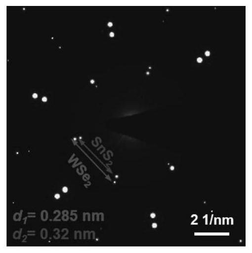
[0137] double-layer SnS 2 / WSe 2 Preparation of vertical heterogeneity:

[0138] Place the porcelain boat filled with S powder in the constant temperature zone upstream of the tube furnace (the temperature is about 180°C, which is the volatilization temperature), and the SnO 2 and tilted wafers (with single-layer WSe 2 nanosheets) porcelain boat placed in the center of the downstream constant temperature zone (temperature is 590 ° C. SnO 2 The mass ratio of powder and S powder is 1:2 (0.05g / 0.1g). Before heating, the air in the quartz tube was purged with 1215 sccm flow rate of argon. Then the constant temperature zones 3 were respectively heated to 590° C. (deposition temperature), and the argon gas flow rate was 120 sccm, and the temperature was kept constant for 8 minutes. There will be a double layer of SnS on the silicon wafer 2 / WSe 2 Vertical heterojunction generation. Generate SnS 2 / WSe 2 The schematic diagram of the vertical heterojunction device is shown i...

Embodiment 2

[0144] Compared with Example 1, the difference is that the volatilization temperature of S powder is 210°C, and the substrate temperature (SnO 2 The volatilization temperature) is 590°C (deposition temperature is 590°C), SnO 2 The mass ratio of powder and S powder is 1:2 (0.05g / 0.1g). The flow rate of Ar is 120 sccm, and the deposition time is 8 min. Figure 11 For the prepared SnS 2 / WSe 2 Optical schematic diagram of a vertical heterojunction, SiO 2 The / Si substrate is light red, and it can be clearly seen that some impurities and defects are generated on the surface of the heterojunction (yellow dots).

Embodiment 3

[0146] Compared with Example 1, the difference is that the S powder volatilization temperature is 150°C, and the substrate temperature (SnO 2 The volatilization temperature) is 590°C (deposition temperature is 590°C), SnO 2 The mass ratio of powder and S powder is 1:2 (0.05g / 0.1g). The flow rate of Ar is 120 sccm, and the deposition time is 8 min. Figure 12 For the prepared SnS 2 / WSe 2 Optical schematic diagram of a vertical heterojunction, SiO 2 / Si substrate is light red, SnS can be seen clearly 2 / WSe 2 The number of heterojunctions is reduced, and most of the samples in the picture are single-layer WSe 2 .


PUM

PropertyMeasurementUnit
volumeaaaaaaaaaa

Abstract

The invention relates to the field of preparation of multi-dimensional high-order superlattices, and particularly discloses a preparation method of a high-order superlattice, which comprises the following steps of: (1) preparing a vertical heterojunction material; and (2) adding a functional solvent to the surface of the vertical heterojunction material within 2 hours from the vertical heterogeneous combination, so as to obtain the high-order superlattice, the functional solvent is an organic solvent-water homogeneous solution; or an organic solvent-water-alkali homogeneous solution. The research of the invention proves for the first time that the high-order Van der Waals superlattice with various material components and sizes can be used for creating a highly engineered structure, thereby exceeding the traditional lattice matching or processing compatibility requirements.

Description

technical field [0001] The invention belongs to the field of nanometer materials, specifically relates to superlattice nanorolls, preparation and application in electricity and magnetoresistance effects, and further proves the universality of the superlattice preparation method. [0002] technical background [0003] The discovery of atomically thin two-dimensional (2D) layered materials opens new avenues for exploring low-dimensional physics at the limit of a single or a few atomic layers, creating a new generation of electronic and optoelectronic devices with unprecedented properties 1-5 . Recently, in addition to studying the intrinsic properties of individual 2D layered atomic crystals, various heterostructures consisting of alternating combinations of individual layered materials such as graphene, hexagonal boron nitride (hBN), and transition metal dichalcogenides (TMDs) , multiple heterostructures, and superlattice structures attract rapidly growing interest among scie...

Claims


Application Information

Patent Timeline
Patent Type & Authority Applications(China)
IPC IPC(8): C30B29/68C30B29/46C30B7/02
CPCC30B29/68C30B29/46C30B7/02Y02P70/50
Inventor 段曦东赵蓓
Owner HUNAN UNIV
Learn More