Solar cell and preparation method thereof

A solar cell and electrode technology, applied in circuits, photovoltaic power generation, electrical components, etc., can solve the problems of reducing the efficiency of heterojunction solar cells and increasing sunlight loss, reducing costs, improving fill factor, and improving photoelectric conversion. The effect of efficiency

Pending Publication Date: 2022-03-22
ZHONGWEI NEW ENERGY CHENGDU CO LTD
View PDF4 Cites 2 Cited by
  • Summary
  • Abstract
  • Description
  • Claims
  • Application Information

AI Technical Summary

Problems solved by technology

If the thickness of the silicon wafer continues to decrease, the wavelength band of the solar spectrum transmission loss will start from a shorter wavelength band (800nm ​​or 700nm), and the loss of sunlight will continue to increase, which will further reduce the efficiency of heterojunction solar cells

Method used


Image

  • Solar cell and preparation method thereof

Examples


preparation example Construction

[0053] Further, the present invention also provides a method for preparing a solar cell as described above, comprising the following steps:

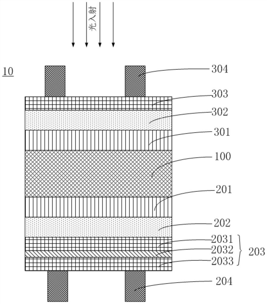
[0054] Step S10: on one side surface of the substrate 100, the first passivation layer 201, the emission layer 202, the first transparent conductive oxide layer 2031, the first conductive metal layer 2032 and the second transparent conductive oxide layer are sequentially stacked and prepared Layer 2033.

[0055] Step S20 : ​​the second passivation layer 301 , the back field layer 302 and the second conductive layer 303 are sequentially stacked on the other surface of the substrate 100 .

[0056] It can be understood that the above step S10 and step S20 are in no particular order, and the other side of the substrate 100 cannot be deposited until one side of the substrate 100 is completed. Specifically, alternate deposition may be performed on the substrate 100 .

[0057] In a specific example, prepare the first passivation layer 201, th...

Embodiment 1

[0074] This embodiment provides a solar cell, the structure of which includes sequentially stacked 20nm silver grid wires as the first electrode, 30nm tin-doped indium oxide (10wt.% tin doping mass percentage) as the second transparent conductive oxide layer, 9nm copper Film as the first conductive metal layer, 30nm tin-doped indium oxide (10wt.% tin doping mass percentage) as the first transparent conductive oxide layer, 12nm B 2 h 6 Amorphous silicon with a doping concentration of 1.5% is used as the emission layer, 8nm intrinsic amorphous silicon is used as the first passivation layer, 150 μm N-type single crystal silicon is used as the substrate, 8nm intrinsic amorphous silicon is used as the second passivation layer, 10nm pH 3 Amorphous silicon with a doping concentration of 2% is used as the back field layer, 80nm tin-doped indium oxide (3 wt.% tin doping mass percentage) is used as the second conductive layer, and 20nm silver grid lines are used as the second electrode...

Embodiment 2

[0078] This embodiment provides a solar cell, the structure of which includes sequentially stacked 20nm silver grid wires as the first electrode, 30nm tin-doped indium oxide (tin-doped mass percentage 10wt.%) as the second transparent conductive oxide layer, 12nm copper Film as the first conductive metal layer, 40nm tin-doped indium oxide (10wt.% tin doping mass percentage) as the first transparent conductive oxide layer, 12nm B 2 h 6 Amorphous silicon with a doping concentration of 1.5% is used as the emission layer, 8nm intrinsic amorphous silicon is used as the first passivation layer, 130 μm N-type single crystal silicon is used as the substrate, 8nm intrinsic amorphous silicon is used as the second passivation layer, 10nm pH 3 Amorphous silicon with a doping concentration of 1.8% is used as the back field layer, 80nm tin-doped indium oxide (3 wt.% tin doping mass percentage) is used as the second conductive layer, and 20nm silver grid lines are used as the second electro...


PUM

PropertyMeasurementUnit
electrical conductivityaaaaaaaaaa
thicknessaaaaaaaaaa
thicknessaaaaaaaaaa

Abstract

The invention provides a solar cell and a preparation method thereof, and the solar cell comprises a substrate, and a first passivation layer, an emission layer and a first conductive layer which are sequentially stacked on the surface of one side of the substrate, wherein the first conductive layer comprises a first transparent conductive oxide layer, a first conductive metal layer and a second transparent conductive oxide layer which are stacked in sequence; according to the solar cell, the first transparent conductive oxide layer, the first conductive metal layer and the second transparent conductive oxide layer which are stacked in sequence are adopted in the first conductive layer, the sandwich structure can effectively reflect sunlight penetrating through the substrate to reach the back transparent electrode, and secondary utilization of light by the heterojunction solar cell is increased; the short-circuit current of the heterojunction cell is further improved; meanwhile, due to the fact that the metal layer is added into the sandwich structure, the conductivity of the sandwich structure is better than that of a traditional transparent conductive oxide thin film, filling factors of the heterojunction solar cell can be effectively improved, and then the photoelectric conversion efficiency of the heterojunction solar cell is improved.

Description

technical field [0001] The invention relates to the technical field of semiconductor devices, in particular to a solar cell and a preparation method thereof. Background technique [0002] Energy is the foundation of the development of human society, and with the development of science and technology, the global demand for energy has surged, making the limitation of traditional energy and its harm to the environment gradually highlighted. In order to solve the problems of environmental pollution and energy crisis in the development process, new energy sources have entered the research field of people, especially solar energy, because of its inexhaustible characteristics and the advantages of no pollution to the environment , has attracted much attention. At present, crystalline silicon cells still occupy the main market of solar cells. Since crystalline silicon cells require many complicated processes in the preparation process to obtain high conversion efficiency, it is di...

Claims


Application Information

Patent Timeline
Patent Type & Authority Applications(China)
IPC IPC(8): H01L31/0224H01L31/054H01L31/0747H01L31/18H01L31/20
CPCH01L31/022425H01L31/022466H01L31/0547H01L31/208H01L31/1884H01L31/0747H01L31/206Y02E10/52Y02P70/50
Inventor 张海川石建华蒙春才袁强付昊鑫杜俊霖孟凡英刘正新
Owner ZHONGWEI NEW ENERGY CHENGDU CO LTD
Why Eureka
Try Eureka