
Silver-tin eutectic thin film solder with copper thin layer introduced and preparation method of silver-tin eutectic thin film solder

A thin-layer and thin-film technology, which is applied in the field of silver-tin eutectic thin-film solder and preparation, can solve the problems that the electrical and thermal properties are difficult to adapt to the development trend of packaging technology, the reliability of solder joints is reduced, and the reliability of solder joints is poor. Reliability and solderability, low cost, and defect reduction effect

Pending Publication Date: 2022-03-29
XI AN JIAOTONG UNIV
View PDF0 Cites 0 Cited by
  • Summary
  • Abstract
  • Description
  • Claims
  • Application Information

AI Technical Summary

Problems solved by technology

The thickness of the solder joint layer obtained by this method is large, and there are many internal pores, which leads to poor reliability of the solder joint, and the electrical and thermal properties are difficult to adapt to the development trend of packaging technology.
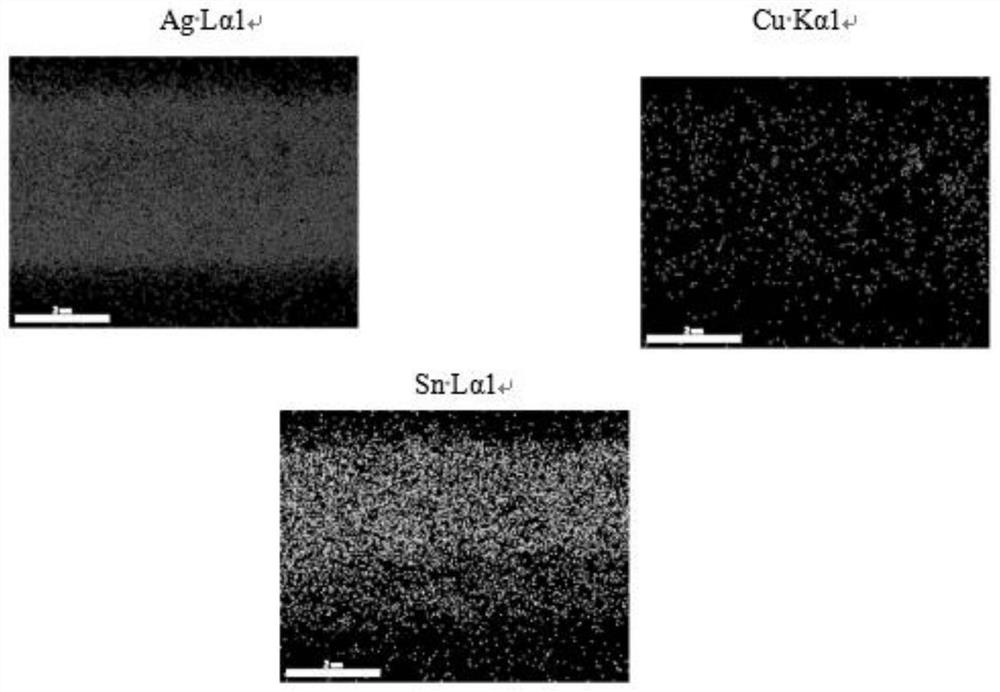
Some studies have prepared silver-tin eutectic thin film solder by magnetron sputtering technology, but due to the serious interdiffusion between silver and tin, the reliability of solder joints has dropped sharply

Method used


Image

  • Silver-tin eutectic thin film solder with copper thin layer introduced and preparation method of silver-tin eutectic thin film solder
  • Silver-tin eutectic thin film solder with copper thin layer introduced and preparation method of silver-tin eutectic thin film solder
  • Silver-tin eutectic thin film solder with copper thin layer introduced and preparation method of silver-tin eutectic thin film solder

Examples


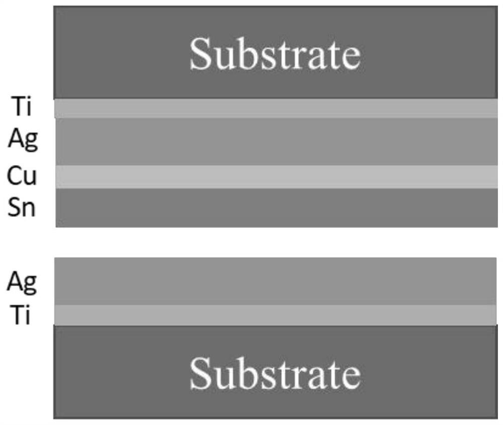
Embodiment 1

[0026] Step 1: Substrate cleaning

[0027] For 6061 aluminum alloy as the substrate material, it was first ultrasonically cleaned in absolute ethanol at 50 Hz for 10 min, then rinsed with deionized water and dried, and then divided into two groups.

[0028] Step 2: Vacuum magnetron sputtering deposition process

[0029] The background vacuum in the magnetron sputtering chamber is 3.0×10 -4 Pa, 20sccm of Ar was introduced, and the working pressure was controlled to be 0.2Pa. Before deposition, the target was pre-sputtered for 10 minutes, and then a group of substrate materials were placed into the sputtering chamber. The DC sputtering power used for silver and copper targets The tin target is 100W, the tin target adopts RF sputtering power of 50W, and the substrate is biased at -50V, and deposits about 1μm silver, 20nm copper and 1μm tin successively. After the deposition is completed, the substrate material is taken out and placed into another set of substrate materials. Dep...

Embodiment 2

[0033] Step 1: Substrate cleaning

[0034] For 6061 aluminum alloy as the substrate material, it was first ultrasonically cleaned in absolute ethanol at 50 Hz for 10 min, then rinsed with deionized water and dried, and then divided into two groups.

[0035] Step 2: Vacuum magnetron sputtering deposition process

[0036] The background vacuum in the magnetron sputtering chamber is 3.0×10 -4 Pa, 30sccm of Ar was introduced, and the working pressure was controlled to be 0.3Pa. Before deposition, the target was pre-sputtered for 10 minutes, and then a group of substrate materials were placed into the sputtering chamber. The silver and copper targets were sputtered by DC sputtering. The power is 130W, the tin target adopts radio frequency sputtering power of 70W, and the substrate is biased at -60V. About 1.5μm silver, 200nm copper and 2μm tin are deposited successively. After the deposition is completed, the substrate material is taken out and placed into another set of substrate...

Embodiment 3

[0040] Step 1: Substrate cleaning

[0041] For SiC ceramics as the substrate material, they were first ultrasonically cleaned in absolute ethanol at 50 Hz for 10 min, then rinsed with deionized water and dried, and then divided into two groups.

[0042] Step 2: Vacuum magnetron sputtering deposition process

[0043] The background vacuum in the magnetron sputtering chamber is 3.0×10 -4 Pa, 40sccm of Ar was introduced, and the working pressure was controlled to be 0.4Pa. Before deposition, the target was pre-sputtered for 10 minutes, and then a group of substrate materials were placed into the sputtering chamber. The silver and copper targets were sputtered by direct current The power is 160W, the tin target adopts radio frequency sputtering power of 120W, the substrate is biased at -80V, and about 2μm silver, 300nm copper and 1.5μm tin are deposited successively. After the deposition is completed, the substrate material is taken out and placed into another set of substrate ma...


PUM

PropertyMeasurementUnit
thicknessaaaaaaaaaa
thicknessaaaaaaaaaa
thicknessaaaaaaaaaa

Abstract

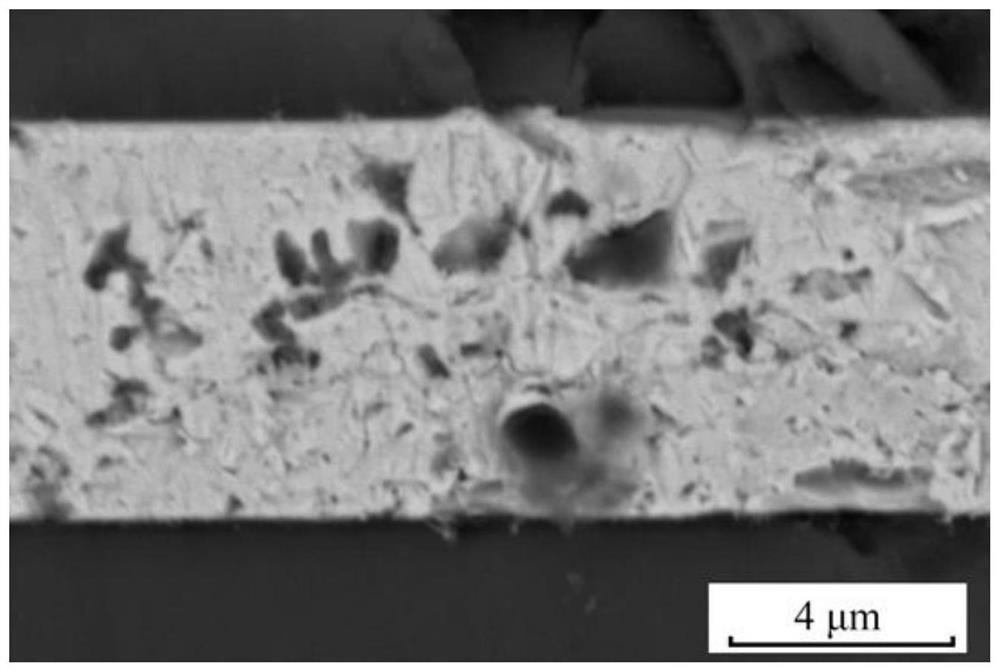
The invention belongs to the technical field of electronic packaging and welding, and discloses a silver-tin eutectic film solder introduced with a copper thin layer, which comprises a copper layer, a silver layer and a tin layer, the silver-tin eutectic film solder introduced with the copper thin layer comprises the following components in percentage by mass: 60-90% of silver, 5-30% of tin and 1-10% of copper, the copper layer is arranged between the silver layer and the tin layer, and the silver layer is not in contact with the tin layer. On the basis of the silver-tin eutectic thin film solder, the copper layer with a certain thickness is introduced between the silver layer and the tin layer, so that the mutual diffusion reaction of silver and tin in the sputtering deposition process can be inhibited, and the copper-tin eutectic thin film solder can be obtained through isothermal solidification volume expansion of a copper-tin intermetallic compound in the high-temperature welding and bonding process. Pores generated by isothermal solidification and shrinkage of the silver-tin intermetallic compound are filled, and defects in a welding layer after welding are reduced, so that the reliability and weldability of a welding spot are improved.

Description

technical field [0001] The invention belongs to the technical field of electronic packaging and welding, in particular to a silver-tin eutectic thin-film solder with a copper thin layer and a preparation method thereof. Background technique [0002] In order to provide mechanical support, protection and heat dissipation paths for components, packaging and interconnection technology needs to be realized by means of soldering. The factors affecting the reliability of solder joints mainly include the type, composition and performance of solder. Traditional solders such as gold-silicon solder and lead-tin solder have excellent wetting properties, ductility and good reliability, and have been widely used in high-temperature process connections. However, the cost of gold is high, and lead is toxic and may cause environmental and health problems. Therefore, the research on lead-free solder has gradually become a research hotspot in the field of electronic packaging. [0003] For t...

Claims


Application Information

Patent Timeline
Patent Type & Authority Applications(China)
IPC IPC(8): H01L23/488H01L21/48B23K20/02B23K35/30C23C14/16C23C14/18C23C14/35
CPCH01L24/29H01L24/27B23K20/023B23K35/3006C23C14/165C23C14/185C23C14/35H01L2224/29083H01L2224/29111H01L2224/29139H01L2224/29147H01L2224/2745
Inventor 宋忠孝杜运达朱晓东李雁淮钱旦王永静
Owner XI AN JIAOTONG UNIV
Learn More