Method for recovering micro-nano copper powder from waste printed circuit board
A technology of printed circuit board and nano copper powder is applied in the field of electronic waste recycling, which can solve the problems of low copper recovery efficiency and complex production process, and achieve the effects of pollution-free, low environmental pollution and wide applicability.
- Summary
- Abstract
- Description
- Claims
- Application Information
AI Technical Summary
Problems solved by technology
Method used
Image
Examples
Embodiment 1
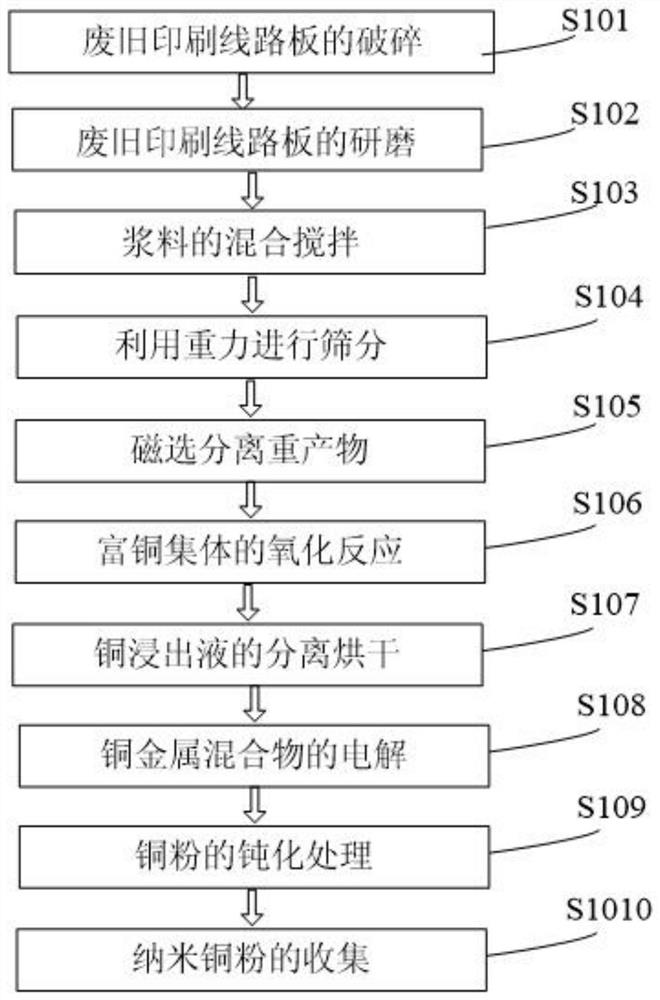
[0071] The invention discloses a method for recovering micronano copper powder from waste printed circuit boards. The specific steps are as follows:
[0072] Step 1: Crushing of waste printed circuit boards; coarsely crushing the waste printed circuit boards with a crusher into pieces smaller than 15cm×15cm, and then crushing them with a strong plastic crusher and a sealed sample preparation grinder to obtain Waste printed circuit board pulverized material, the particle size of the waste printed circuit board pulverized material is ≤30 mesh;
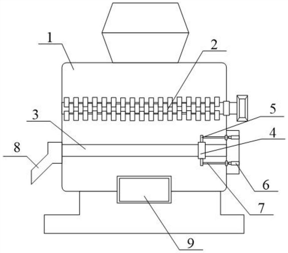
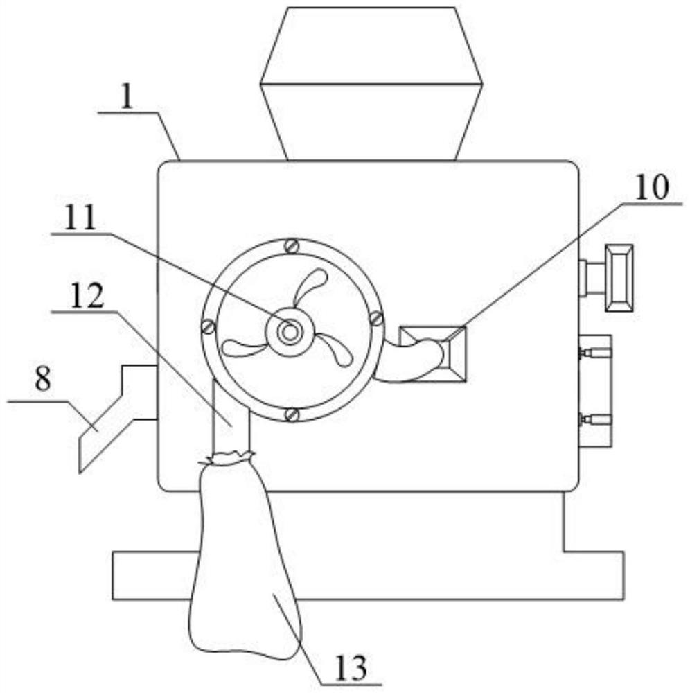
[0073] Step 2: Grinding of waste printed circuit boards; the small pieces of material obtained by the preliminary shearing in step 1 are sent to the cutting grinder, and in the cutting grinder, the blades rotating at high speed further crush the small pieces of material to obtain a particle size smaller than 10mm fine-grained material;
[0074] Step 3: mixing and stirring the slurry; sending the fine-grained material in step 2 and an ap...
Embodiment 2
[0083] The invention discloses a method for recovering micronano copper powder from waste printed circuit boards. The specific steps are as follows:
[0084] Step 1: Crushing of waste printed circuit boards; coarsely crushing the waste printed circuit boards with a crusher into pieces smaller than 15cm×15cm, and then crushing them with a strong plastic crusher and a sealed sample preparation grinder to obtain Waste printed circuit board pulverized material, the particle size of the waste printed circuit board pulverized material is ≤30 mesh;
[0085] Step 2: Grinding of waste printed circuit boards; the small pieces of material obtained by the preliminary shearing in step 1 are sent to the cutting grinder, and in the cutting grinder, the blades rotating at high speed further crush the small pieces of material to obtain a particle size smaller than 10mm fine-grained material;
[0086] Step 3: mixing and stirring the slurry; sending the fine-grained material in step 2 and an ap...
PUM
| Property | Measurement | Unit |
|---|---|---|
| particle size | aaaaa | aaaaa |
| particle size | aaaaa | aaaaa |
| particle diameter | aaaaa | aaaaa |
Abstract
Description
Claims
Application Information


