Hot carrier bidirectional separation type p-i-n type two-dimensional heterojunction, preparation method and device

A p-i-n, two-dimensional heterojunction technology, applied in the field of hot carrier bidirectional separation type p-i-n type two-dimensional heterojunction and preparation, can solve the problem that the interaction between light and matter is not strong enough, and the photocurrent of photogenerated carriers is reduced. , the interface is not clean enough, etc., to achieve the effect of easy to achieve large-scale sample preparation, solve the bubble generation, and facilitate device integration

Pending Publication Date: 2022-04-12
HUAZHONG UNIV OF SCI & TECH
View PDF0 Cites 0 Cited by
  • Summary
  • Abstract
  • Description
  • Claims
  • Application Information

AI Technical Summary

Problems solved by technology

[0005] (1) Due to the thickness limitation, the width of the depletion region is narrow, and the diffusion of photogenerated carriers will lead to a decrease in photocurrent;
[0006] (2) Due to thickness limitations, the interaction between light and matter is still not strong enough, and the absorption of light is far lower than the ideal absorption;
[0007] (3) At present, the main construction method is still transfer, and its interface is not clean enough

Method used


Image

  • Hot carrier bidirectional separation type p-i-n type two-dimensional heterojunction, preparation method and device
  • Hot carrier bidirectional separation type p-i-n type two-dimensional heterojunction, preparation method and device
  • Hot carrier bidirectional separation type p-i-n type two-dimensional heterojunction, preparation method and device

Examples


Embodiment 1

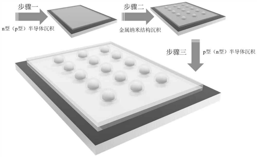
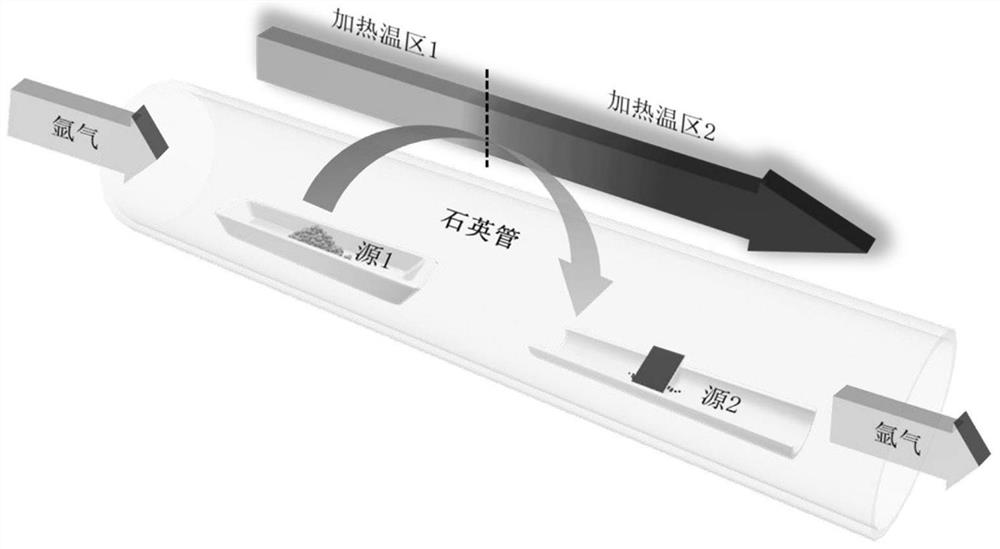
[0040] The present invention prepares a kind of n-MoS 2 / Au / p-WS2 Heterojunction. figure 2 It shows the reaction equipment and process. see Figure 1-3 , the preparation method specifically includes the following steps:

[0041] (1) Step 1: Chemical vapor deposition of n-type semiconductor material on the substrate. A three-zone horizontal tube furnace was used as the reaction vessel. A silicon wafer with a 300nm thick oxide layer on one side is selected as the substrate. MoO will be used as metal source 2 Mix the powder and NaCl powder as a growth aid at a mass ratio of 50:1 and grind thoroughly, weigh 1-2 mg of the mixture and put it into a U-shaped groove, place the side of the silicon wafer with the oxidized layer facing the source, and place it above the source. , put the U-shaped groove in the heating center. The S powder is placed in the upstream of the U-shaped groove away from the heating center, and the middle temperature zone is raised to a growth temperatur...

Embodiment 2

[0045] The present invention prepares a kind of n-MoSe 2 / Au / p-WSe 2 Heterojunction. The preparation method specifically comprises the following steps:

[0046] Repeat Example 1 with the described steps, the difference is that the non-metallic source of chemical vapor deposition is Se powder for the first time, and the holding temperature in the middle temperature zone is set to 850°C; the non-metallic source of chemical vapor deposition for the second time is Se powder, and the middle holding The temperature was set to 950°C.

Embodiment 3

[0048] The present invention prepares a kind of p-NiO / Ag / n-MoS 2 Heterojunction. The preparation method specifically comprises the following steps:

[0049] (1) Step 1: magnetron sputtering. Si(111) is selected as the substrate, and Ni with a purity of 99.999% is used as the target. Vacuumize until the vacuum degree in the chamber reaches 1.0×10 -5 After Pa, open the inflation valve, feed the carrier gas Ar with a flow rate of 20 sccm, and adjust the air pressure to 0.5 Pa after the air pressure in the chamber is stabilized. Debug the sputtering parameters, and turn on the power for 5 minutes of pre-sputtering without opening the baffle. After the pre-sputtering is completed, the reaction gas O is introduced into the chamber 2 , the flow rate is 5sccm. After the air pressure in the chamber is stabilized, adjust the air pressure to 0.5Pa. After the air pressure stabilized, open the baffle to start sputtering. After the sample is cooled, fill the chamber with air and tak...


PUM

PropertyMeasurementUnit
thicknessaaaaaaaaaa
thicknessaaaaaaaaaa

Abstract

The invention discloses a hot carrier bidirectional separation type p-i-n type two-dimensional heterojunction, a preparation method and a device. The heterojunction is of a sandwich structure and comprises an n-type semiconductor material, metal with a nano structure and a p-type semiconductor material from bottom to top. Or the heterojunction comprises the p-type semiconductor material, the metal with the nano structure and the n-type semiconductor material from bottom to top. The preparation method comprises the following steps: depositing a layer of n-type semiconductor material on the surface of a substrate; depositing a layer of metal with a nano structure on the surface of the n-type semiconductor material by adopting a physical vapor deposition mode; and depositing a layer of p-type semiconductor material on the metal surface with the nano structure. According to the invention, Schottky junctions are respectively formed by the metal of the nanostructure arranged in the middle and the p-type semiconductor and the n-type semiconductor, so that the generation, transmission and collection efficiency of current carriers is effectively improved, and the light absorption is improved.

Description

technical field [0001] The invention belongs to the technical field of preparation of two-dimensional nanomaterials and optoelectronic devices, and more specifically relates to a hot carrier bidirectional separation type p-i-n type two-dimensional heterojunction, a preparation method and a device. Background technique [0002] Layered semiconductor materials with a two-dimensional crystal structure have excellent electronic, optical, and mechanical properties, and are widely used in the research of optoelectronic devices, and are expected to be applied in biosensing, photodetection and other fields. Their thickness is one to several atomic layers thick, which can effectively avoid the short channel effect caused by the reduction of the device scale, and have semiconductor characteristics, or are expected to be the basis of the next generation of semiconductor devices. The ideal two-dimensional interface with atomic thickness and atomic level is also the biggest advantage of ...

Claims


Application Information

Patent Timeline
Patent Type & Authority Applications(China)
IPC IPC(8): H01L31/18H01L31/105C23C14/08C23C14/16C23C14/30C23C14/35C23C16/30C23C28/00
CPCY02P70/50
Inventor 李渊欧阳德才刘盛洪翟天佑
Owner HUAZHONG UNIV OF SCI & TECH
Why Eureka
Try Eureka