Check patentability & draft patents in minutes with Patsnap Eureka AI!

A kind of aluminum gallium nitride based ultraviolet light emitting diode epitaxial layer structure and preparation method thereof

A light-emitting diode, AlGaN technology, applied in semiconductor devices, electrical components, circuits, etc., can solve the problems of difficult doping, low luminous efficiency, and high density of AlGaN-based thin films, so as to improve doping and injection efficiency, and improve luminescence. Efficiency, the effect of improving the quality of epitaxial crystals

Active Publication Date: 2022-07-12
CHANGSHU INSTITUTE OF TECHNOLOGY
View PDF2 Cites 0 Cited by
  • Summary
  • Abstract
  • Description
  • Claims
  • Application Information

AI Technical Summary

Problems solved by technology

[0005] In view of the above-mentioned defects in the prior art, the task of the present invention is to provide an epitaxial layer structure of an AlGaN-based ultraviolet light-emitting diode, which solves the problems of excessively high defect density, difficult doping, and generally low luminous efficiency in the AlGaN-based thin film. , increase the concentration of carriers in the n-region and p-region and the efficiency of injection into the quantum well region, and improve the light extraction efficiency of the device

Method used


Image

  • A kind of aluminum gallium nitride based ultraviolet light emitting diode epitaxial layer structure and preparation method thereof
  • A kind of aluminum gallium nitride based ultraviolet light emitting diode epitaxial layer structure and preparation method thereof
  • A kind of aluminum gallium nitride based ultraviolet light emitting diode epitaxial layer structure and preparation method thereof

Examples


Embodiment 1

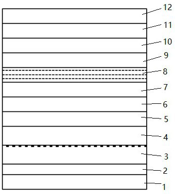
[0041] Example 1, please combine figure 1 As shown, the structure of the epitaxial layer of the AlGaN-based UV light emitting diode in this embodiment is as follows: it includes a sapphire substrate 1, a nucleation layer 2, an Al x1 Ga 1-x1 N transition layer 3, Al x2 Ga 1-x2 N buffer layer 4, Al x3 Ga 1-x3 N buffer layer 5, Al x4 Ga 1-x4 N buffer layer 6, n-type Al x5 Ga 1-x5 N layer 7, Al x6 Ga 1-x6 N / Al x7 Ga 1-x7 N multiple quantum well layer 8, p-type Al x8 Ga 1-x8 N electron blocking layer 9, p-type Al x9 Ga 1-x9 N layer 10, p-type Al x10 Ga 1-x10 N layer 11 and p-type Al x11 Ga 1-x11 N layer 12 .

[0042] please combine figure 2 shown, wherein, the sapphire substrate 1 is a double-sided polished C-plane crystal, Al x1 Ga 1-x1 The surface of the N transition layer 3 away from the sapphire substrate 1 is uniformly provided with a nanoscale cavity structure in a matrix arrangement. The nanoscale cavity structure is an inverted conical cavity 13a, an...

Embodiment 2

[0059] Example 2, the stacked structure of the AlGaN-based UV light emitting diode epitaxial layer in this example is the same as that in Example 1, wherein the sapphire substrate is a double-sided polished C-plane crystal, and nano-scale convex structures are prepared on the surface of the sapphire substrate , the nano-scale convex structure is a cylinder 14, the bottom diameter of the cylinder 14 is 30 nm, the geometric center distance of the adjacent cylinders 14 is 10-50 nm, and the height of the cylinder 14 is 30 nm. please combine Figure 4 shown, Al x1 Ga 1-x1 The side of the N transition layer away from the sapphire substrate is uniformly arranged with a nanoscale cavity structure in a matrix arrangement. The nanoscale cavity structure is a hexagonal living cavity 13b, and the longitudinal cross-sectional depth of the hexagonal column cavity 13b is 1 nm. The geometric center distance of the hexagonal prism cavity 13b is 5nm, and the distance of the top surface openin...

Embodiment 3

[0062] Embodiment 3, the stacked structure of the AlGaN-based UV light emitting diode epitaxial layer in this embodiment is the same as that of Embodiment 1, wherein, Al x1 Ga 1-x1 The side of the N transition layer away from the sapphire substrate is uniformly arranged with inverted conical cavities in a matrix arrangement. The longitudinal section depth of the inverted conical cavities is 2 nm, and the geometric center spacing of adjacent inverted conical cavities is 3 nm. The maximum opening distance (diameter in this example) of the top surface of the cavity is 3 nm. The nucleation layer is AlN with a thickness of 100 nm, Al x1 Ga 1-x1 The thickness of the N transition layer is 1000 nm, the Al x2 Ga 1-x2 The thickness of the N buffer layer is 1000 nm, the Al x3 Ga 1-x3 The thickness of the N buffer layer is 500 nm, the Al x4 Ga 1-x4 The thickness of the N buffer layer is 300 nm, and the n-type Al x5 Ga 1-x5 The thickness of the N layer is 1000 nm, Al x6 Ga 1-x6...


PUM

PropertyMeasurementUnit
thicknessaaaaaaaaaa
thicknessaaaaaaaaaa
thicknessaaaaaaaaaa

Abstract

The invention discloses an aluminum gallium nitride-based ultraviolet light emitting diode epitaxial layer structure, which comprises a sapphire substrate, a nucleation layer, an Al x1 Ga 1‑x1 N transition layer, Al x2 Ga 1‑x2 N buffer layer, Al x3 Ga 1‑x3 N buffer layer, Al x4 Ga 1‑x4 N buffer layer, n-type Al x5 Ga 1‑x5 N layer, Al x6 Ga 1‑x6 N / Al x7 Ga 1‑x7 N multiple quantum well layer, p-type Al x8 Ga 1‑x8 N electron blocking layer, p-type Al x9 Ga 1‑x9 N layer, p-type Al x10 Ga 1‑x10 N-layer and p-type Al x11 Ga 1‑x11 N layer, the Al x1 Ga 1‑x1 The surface of the N transition layer away from the sapphire substrate is uniformly provided with a nanoscale cavity structure, 0<x1≤x2<x3≤x4≤x5<1, 0<x11<x10≤x9≤x8<1, 0<x7< x5≤x6<1, x9≤x5. The invention also discloses a preparation method of the epitaxial layer structure of the aluminum gallium nitride-based ultraviolet light emitting diode. The aluminum gallium nitride-based ultraviolet light emitting diode epitaxial layer structure of the present invention solves the problems of excessively high defect density, difficult doping and generally low luminous efficiency in the AlGaN-based thin film, and improves the light extraction efficiency.

Description

technical field [0001] The invention relates to an ultraviolet diode epitaxial layer structure and a preparation method thereof, in particular to an aluminum gallium nitride-based ultraviolet light emitting diode epitaxial layer structure and a preparation method thereof. Background technique [0002] Aluminum Nitride Gallium (AlGaN)-based semiconductor materials are direct bandgap wide-gap semiconductor materials, which have broad application prospects in air purification, biomedical, and defense industries, and are key basic materials for high-quality UV LEDs. ternary compound Al x Ga 1-x The energy band gap of N can be adjusted by changing the Al composition x, so that the corresponding wavelength is continuously adjustable between 200 and 365 nm. [0003] However, unlike gallium nitride (GaN)-based blue-green LEDs, the fabrication of high-quality AlGaN materials becomes increasingly difficult as the emission wavelength becomes shorter, that is, the aluminum composition...

Claims


Application Information

Patent Timeline
Patent Type & Authority Patents(China)
IPC IPC(8): H01L33/06H01L33/12H01L33/14H01L33/22H01L33/32H01L33/00
Inventor 王书昶娄祎祎刘玉申丁恒姜文琪牛信睿
Owner CHANGSHU INSTITUTE OF TECHNOLOGY
Features
  • R&D
  • Intellectual Property
  • Life Sciences
  • Materials
  • Tech Scout
  • Unparalleled Data Quality
  • Higher Quality Content
  • 60% Fewer Hallucinations
Learn More