
Narrow-band-gap semiconductor device and preparation method thereof

A semiconductor, narrow bandgap technology, applied in the fields of semiconductor devices, semiconductor/solid-state device manufacturing, electrical components, etc., can solve the problems of large alignment deviation, complex structure preparation, difficult integration, etc., to suppress the bipolar problem of the device , The production process is simple and efficient, and the effect of solving the problem of static power consumption

Pending Publication Date: 2022-05-03
BEIJING INST OF CARBON BASED INTEGRATED CIRCUIT +1
View PDF0 Cites 0 Cited by
  • Summary
  • Abstract
  • Description
  • Claims
  • Application Information

AI Technical Summary

Problems solved by technology

However, due to the small bandgap, when working in the off state, the minority carrier tunneling at the drain is very serious
In addition, this kind of feedback gate also has many shortcomings in the process. Because it adopts a non-self-aligned process, there is a large alignment deviation problem, and it is not compatible with the current integrated circuit manufacturing process, so it cannot be mass-produced.
In addition, the drain terminal occupies a large contact area, and it is difficult to continue to shrink with the development of semiconductor technology nodes.
[0007] In addition, IBM reported an asymmetric contact structure, which widens the Schottky barrier into a triangular barrier by etching near the drain end, thereby increasing the switching ratio. However, the drain end barrier of this method There is still a thinning trend with increasing bias voltage
In addition, this method is also a non-self-alignment process, which has alignment problems, and the structure is complicated to prepare and the controllability of wet etching is poor. The uniformity and stability of device performance are challenged, and it is not easy to integrate.

Method used

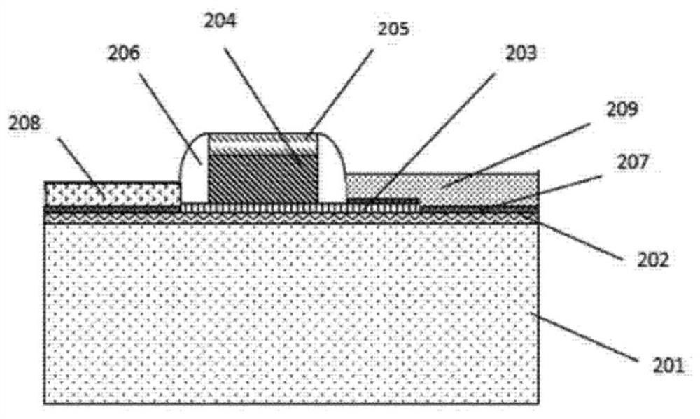
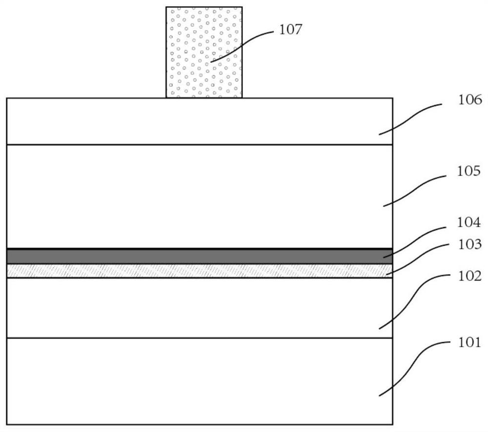
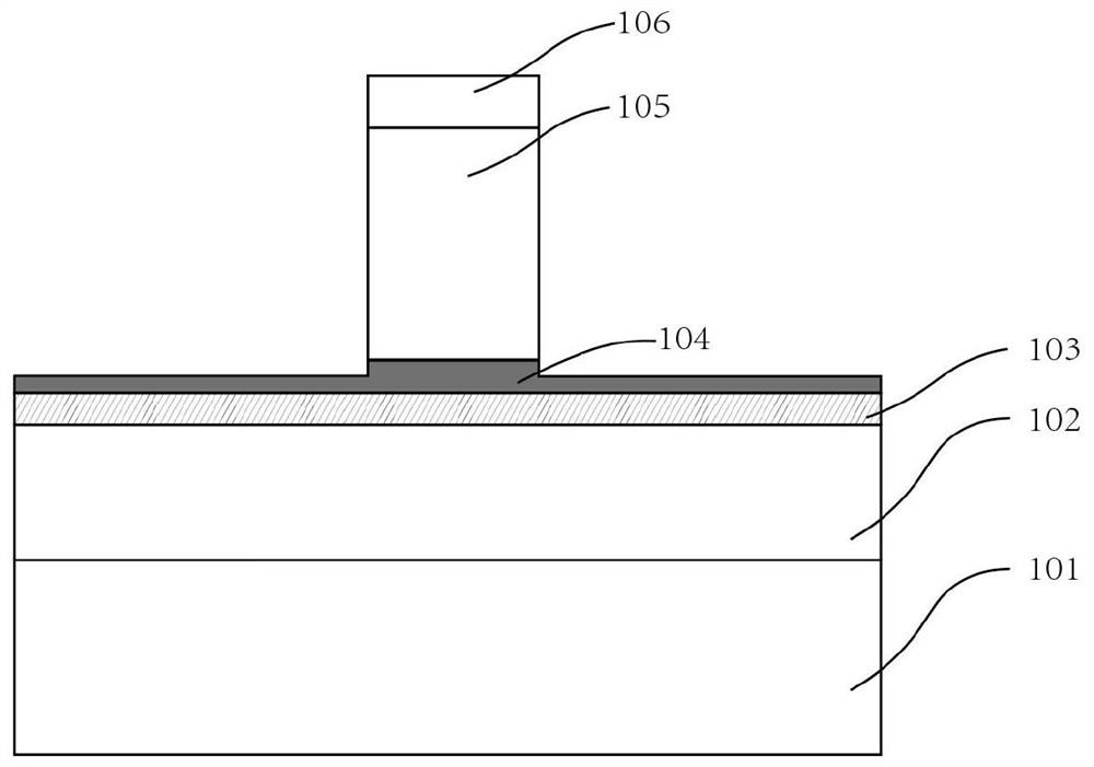

Image

  • Narrow-band-gap semiconductor device and preparation method thereof
  • Narrow-band-gap semiconductor device and preparation method thereof
  • Narrow-band-gap semiconductor device and preparation method thereof

Examples


Embodiment Construction

[0059] Embodiments of the present invention will be described in detail below with reference to the accompanying drawings. In the various drawings, the same elements are denoted by the same reference numerals, and various parts in the drawings are not drawn to scale. Also, some well-known parts may not be shown. For the sake of simplicity, the semiconductor structure obtained after several steps can be described in one figure.

[0060] It should be understood that when describing the structure of a device, when a layer or a region is referred to as being "on" or "over" another layer or another region, it may mean being directly on another layer or another region, or Other layers or regions are also included between it and another layer or another region. And, if the device is turned over, the layer, one region, will be "below" or "beneath" the other layer, another region.

[0061] If it is to describe the situation directly on another layer or another area, the expression "...


PUM

PropertyMeasurementUnit
thicknessaaaaaaaaaa
thicknessaaaaaaaaaa
band gapaaaaaaaaaa

Abstract

The invention provides a narrow-band-gap semiconductor device with a high switch ratio and a manufacturing method of the narrow-band-gap semiconductor device. The device is provided with a supporting substrate, a narrow-band-gap semiconductor layer, a gate dielectric layer and a gate stacking structure are sequentially arranged on the supporting substrate, and L-shaped self-alignment side walls are arranged on the two sides of the gate stacking structure. And the horizontal part and the gate dielectric layer below the horizontal part respectively extend towards the source region and the drain region at the outer side for a certain length along the plane where the narrow-band gap semiconductor layer is located. Metal is further deposited on the horizontal part of the outer side of the side wall and the narrow-band-gap semiconductor layer, and the narrow-band-gap semiconductor layer is used as a source electrode and a drain electrode of the semiconductor device. According to the device, a side wall is formed through a grid electrode self-alignment technology, the electric field intensity at the junction of a channel and a source and drain electrode region can be reduced, the width of a tunneling potential barrier between drain electrode end bands is increased, reverse tunneling of drain electrode end minority carriers can be well restrained when the device works under large bias voltage, and the reliability of the device is improved. Therefore, the switching ratio can be increased while the high performance of the narrow-band-gap semiconductor device is maintained, and the bipolar is remarkably suppressed.

Description

technical field [0001] The invention relates to a semiconductor device and a manufacturing method thereof, in particular to a field-effect transistor with carbon nanotubes and a manufacturing method thereof. Background technique [0002] At present, the feature size of key patterns of advanced silicon-based integrated circuit devices has crossed the 10nm mark. When transistors continue to develop to 5nm or even smaller node technology, it is foreseeable that silicon-based semiconductor technology is being affected by processing technology, device physics Limit, performance and other challenges, its continued development must overcome huge obstacles in terms of power consumption and cost, and the development space is becoming smaller and smaller. It is urgent to find new information devices to continue to promote the development of the future semiconductor industry. [0003] In recent years, many new semiconductor materials have great development potential in the field of hig...

Claims


Application Information

Patent Timeline
Patent Type & Authority Applications(China)
IPC IPC(8): H01L29/78H01L29/06H01L21/336H01L29/423
CPCH01L29/78H01L29/0603H01L29/0684H01L29/66477H01L29/42356
Inventor 孟令款张志勇彭练矛
Owner BEIJING INST OF CARBON BASED INTEGRATED CIRCUIT
Learn More