Check patentability & draft patents in minutes with Patsnap Eureka AI!

Deep ultraviolet microscope imaging objective lens

An imaging objective lens and microscope technology, applied in the field of microscope imaging objective lens, can solve problems such as high cost and complicated manufacturing process, and achieve the effects of reducing manufacturing cost, simplifying structure, and reducing the number of sheets

Pending Publication Date: 2022-05-06
FUDAN UNIV
View PDF7 Cites 0 Cited by
  • Summary
  • Abstract
  • Description
  • Claims
  • Application Information

AI Technical Summary

Problems solved by technology

The general deep ultraviolet defect imaging objective lens contains about 20 lenses, and the tube lens working with it contains 3 objective lenses, and works at a wavelength of 238~266 nm or above, with a numerical aperture of 0.9 or below, and its resolution is 66 nm and a half cycle, the manufacturing process is complicated, and the cost is high

Method used


Image

  • Deep ultraviolet microscope imaging objective lens
  • Deep ultraviolet microscope imaging objective lens

Examples


Embodiment 1

[0023] The idea of ​​this design is to use a combination of positive and negative lenses to eliminate spherical aberration and field curvature, and to use a symmetrical configuration in which the objective lens and the tube lens are separated on both sides of the pupil to improve the detection of coma, astigmatism, distortion, and lateral chromatic aberration. Poor elimination ability. Optical resolution formula, as shown in formula (1):

[0024] (1)

[0025] Among them, HP (Half Pitch) represents the half period, lambda represents the wavelength, and NA (Numerical Aperture) represents the numerical aperture. For example [Document 1]: lambda=248 nm, NA=0.9, then HP=69 nm. Another example is this design: lambda=193nm, NA=0.8, then HP=60 nm.

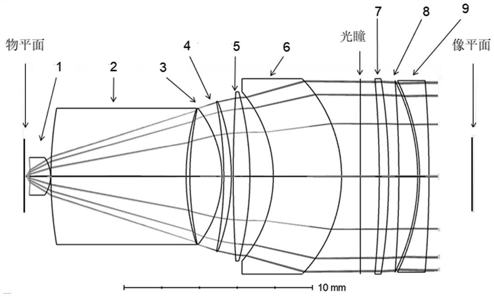
[0026] figure 1 It is a schematic diagram of the overall structure of an implementation of the objective lens of the present invention. The first lens 1, the second lens 2, the third lens 3, the fourth lens 4, the fifth lens 5 and...


PUM

PropertyMeasurementUnit
lengthaaaaaaaaaa
lengthaaaaaaaaaa

Abstract

The invention discloses a deep ultraviolet microscope imaging objective lens. The lens is cooperated with the barrel lens; the equivalent numerical aperture is 0.75-0.85, the working wavelength is 190-200 nm, the equivalent focal length is 3-8 mm, and the magnifying power is 100-200 times; the six spherical lenses are sequentially arranged along an optical axis and are respectively a first lens, a second lens, a third lens, a fourth lens, a fifth lens and a sixth lens, the first lens, the third lens, the fourth lens and the fifth lens are positive lenses, and the second lens and the fourth lens are negative lenses; the barrel lens cooperatively working with the lens body comprises three objective lenses; the objective lens provided by the invention can be applied to defect detection of a patterned silicon wafer of a semiconductor integrated circuit, and the defect detection resolution can reach 58-64 nanometers or smaller.

Description

technical field [0001] The invention belongs to the technical field of integrated circuit manufacturing, and in particular relates to a deep ultraviolet microscope imaging objective lens. Background technique [0002] The manufacturing of semiconductor integrated circuits has entered the deep sub-micron line width, and the defects in the manufacturing process have an increasing impact on the performance and yield of integrated circuits. In the process flow of semiconductor integrated circuits, the effective control of defects is the key to ensure the yield and performance. In terms of defect detection, optical imaging detection is the main and fast method. Since the detection sensitivity and resolution depend on the optical resolution, the shorter the wavelength or the larger the numerical aperture, the higher the resolution. As the line width of integrated circuit manufacturing continues to shrink, the manufacturing density of integrated circuits is increasing, and there ...

Claims


Application Information

Patent Timeline
Patent Type & Authority Applications(China)
IPC IPC(8): G02B21/02G02B21/16G02B13/00G02B1/11
CPCG02B21/02G02B21/16G02B13/00G02B1/11
Inventor 伍强李艳丽刘显和
Owner FUDAN UNIV
Features
  • R&D
  • Intellectual Property
  • Life Sciences
  • Materials
  • Tech Scout
  • Unparalleled Data Quality
  • Higher Quality Content
  • 60% Fewer Hallucinations
Learn More